BPM1527SJ Datasheet Deep Dive: Key Specs & Metrics
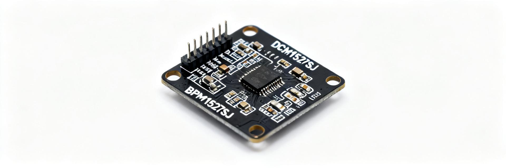
Modern isolated DC/DC power modules routinely reach high full-load efficiencies and sub-100 mW standby draws. This analysis extracts the BPM1527SJ datasheet essentials to surface key specs for system integration and verification. Background: What the BPM1527SJ Is and Where It Fits BPM1527SJ VCC GND OUT+ OUT- ISOLATION BARRIER Product Class & Intended Role The BPM1527SJ is an isolated DC/DC converter intended for compact auxiliary supplies. It excels in the single-digit watt class where space, isolation, and low standby power are primary requirements. Application Typical Requirement Industrial Control 4 W, reinforced isolation, wide Vin Telecom Auxiliary Small footprint, low standby, surge tolerance Consumer ITE Low cost, compact, EMI control Electrical Key Specs: Input, Output & Efficiency Input-Side Parameters Read absolute maximum ratings and recommended Vin first. Use these values to size upstream fuses and TVS devices. Plan start-up sequencing per recommended Vin ramp to avoid latch-up events. Output & Efficiency Profile Extract nominal Vout, max Iout, and ripple limits. Example: If Vout=5.0V at Iout=0.8A (4.0W) with 88% efficiency, input power is ~4.545W, requiring 0.55W of thermal dissipation via the PCB. Thermal, Reliability & Protection Metrics Locate thermal resistance and ambient derating curves. Target 70–80% of rated output at worst-case ambient. Protections like OCP and OTP drive your layout and test strategy, defining creepage and clearance requirements. Practical Bench Test Plan Input Sweep: Verify start-up and no-load standby power. Output Regulation: Measure Vout, ripple, and efficiency from 0–100% load. Thermal Imaging: Compare junction/ambient margins at full load. Protection Triggering: Confirm safe restart after OCP/OVP events. Actionable Design Checklist Confirm Vin range and Vout tolerance against electrical tables. Compare expected module loss to datasheet derating curves. Validate OCP/OVP behavior under controlled conditions. Verify isolation test plan (hipot/insulation resistance). Ensure input bulk and output decoupling caps meet ESR specs. Common Questions & Answers Is the BPM1527SJ suitable for a 4W isolated auxiliary supply? It can be suitable if the datasheet’s max output current and derating curves support 4 W at your worst-case ambient. Verify efficiency at intended load and ensure thermal margin with PCB copper and vias. How should I verify the BPM1527SJ efficiency and thermal performance? Run an input sweep and stepped-load efficiency test with a power meter. Stabilize at worst-case load for thermal imaging and compare measured temperature rise to datasheet curves. What are the primary datasheet key specs to reference for PCB layout and EMI? Reference isolation voltage, creepage/clearance, and recommended external components. Place input caps close to pins, separate primary/secondary copper, and add thermal vias. What are common failure modes and mitigations? Common modes include overtemp (mitigated by thermal headroom) and excessive ripple (mitigated by low-ESR decoupling). Always validate safety gates through lab functional tests. Summary Track these critical datapoints: permitted input range, nominal output rating, efficiency vs. load, and isolation rating. Immediate next steps: perform bench validation and confirm PCB thermal layout against the datasheet specs.