
Comprehensive technical analysis of the automotive-grade single non-inverting buffer with open-drain output.
The 74LVC1G07GW-Q100 is a single non-inverting buffer with an open-drain output designed for mixed-voltage systems and demanding environments. Key datasheet figures frame its usefulness: wide VCC support from 1.65–5.5 V, very low standby ICC in the microampere range, open-drain output capable of sourcing external pull-ups and sinking up to ~32 mA, and an extended ambient rating down to −40°C and up to +125°C for automotive-grade robustness. This article walks through the 74LVC1G07GW-Q100 datasheet to explain pinout, electrical characteristics, integration tips, and troubleshooting guidance for practical designs.
Readers will get a pin-by-pin description, package and soldering notes, DC and AC parameter interpretation, layout and pull-up resistor guidance, thermal and qualification considerations, plus a compact pre-deployment checklist. The aim is practical application: selecting pull-ups and decoupling, estimating timing with given propagation delays and capacitive loads, and avoiding common pitfalls when the part is used as a level-shifting open-drain buffer on shared buses.
Background & Device Overview
Core Functionality
The part is a single non-inverting buffer with an open-drain output used to gate and isolate logic signals. The open-drain topology means the device actively pulls the line low but relies on an external pull-up for a defined high level. This enables wire-OR logic, level translation between different VCC domains, and shared-bus operation.
Key Selling Points
The datasheet highlights low-voltage operation, broad VCC range, and automotive-level qualification. Typical ICC in standby is in the microampere class, and IO sink capability approaches several tens of milliamps. Q100-style qualification implies extra screening and extended-temperature robustness.
Pinout & Package Details
Pin-by-Pin Description
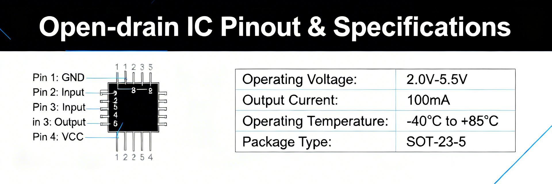
The five-pin package pin mapping is straightforward: VCC, GND, input (A), output (Y open-drain), and any NC or substrate ties as specified. For documentation and PCB silkscreen, ensure the orientation notch is clearly identified to prevent assembly errors.
Electrical Characteristics: DC and AC Specs
Operating Voltage Visualization (VCC)
Before selection, verify supply range, absolute-max ratings, logic thresholds, and leakage. Operating VCC is 1.65–5.5 V; absolute max VCC and thermal limits must be respected. When using pull-ups, remember the added RC time constant from the resistor and bus capacitance slows edges; select pull-ups to balance required edge speed and static current.
Integration & Design Recommendations
⚡ Power & Layout
- • Use a 0.1 μF ceramic decoupling capacitor close to the VCC pin.
- • Keep input and output traces as short as possible.
- • Route sensitive lines away from high-current traces.
🔗 Pull-up Selection
Pull-ups define high-level voltage and edge speed. Use R = (VCC − VOL_max)/I_pull as a guide.
• 10 kΩ – 100 kΩ: Low power, static logic
• 2.2 kΩ – 10 kΩ: High speed (3.3V/5V)
Thermal & Automotive Reliability
Calculate power dissipation (Pd = ICC*VCC + Iout*Vdrop) to assess thermal margin. For automotive applications, the Q100-style qualification implies additional screening and suitability for extended temperature ranges. Account for extended temp drift in thresholds and possibly tighter derating for long-life reliability in harsh environments.
Testing & Troubleshooting Checklist
Common Issues
- ❌ No output (Missing pull-up)
- ❌ Slow edges (High bus capacitance)
- ❌ High current (IO limit exceeded)
Pre-Deployment Checklist
- ✅ Verify pin 1 orientation
- ✅ Confirm VCC is 1.65V-5.5V
- ✅ Validate pull-up resistor value
Summary
The 74LVC1G07GW-Q100 is a compact open-drain single buffer ideal for level translation, shared-bus designs, and low-power systems where small packages and automotive-grade robustness are required. Critical items to watch are the VCC operating range, correct pull-up strategy, and the IO sink limits under worst-case scenarios. For integration, prioritize local decoupling, short trace runs, and calculated pull-up choices that balance rise time against static current. Consult the manufacturer datasheet for final sign-off and validate with a prototype run before volume release.


