


Helping you save cost and time.

Provide reliable packaging for your goods.

Quick and reliable delivery to save time.

Excellent after-sales service.
New Product Launch
More +

Hot Selling Parts

| Manufacturer | Part Number |
|---|---|
| 村田 | BLM18AG102SN1D |
| TOSHIBA/TOSHIBA | TCD2709DG |
| NEC | SF152Y |
| AVX | FR10560N0050JBK |
| DIODES | ABS10A-13 |
| OSRAM | LEUWD1W101-7L-HM-0-700 |
| EL | EL6257CU |
| SULLINS | SBH11-PBPC-D07-ST-BK |
| Manufacturer | Part Number |
|---|---|
| RFMD | RF1694TR13-5K |
| BOURNS | SRP1245A-180M |
| MCN | MT46V32M8TG-6TIT:G |
| EXAR | XRT7298IW |
| KE | DSIC03LSGET |
| MOLEX | 0512810894 |
| H | SMCJ70CA-HCA1 |
| PTTR | KRPA-11AN-12 |
| Manufacturer | Part Number |
|---|---|
| OMRON | XH5B-1215-5N |
| OMRON | XW4H-11A1 |
| OSRAM | SFH2400FA |
| ON | 1SMB5918BT3G |
| NEXPERIA/安世 | PMEG10010ELRX |
| AAP2968-28VIR1 | |
| TE | 5-146280-6 |
| TE | YACT20JD19PNC00100A |
| Manufacturer | Part Number |
|---|---|
| ALLIANCE | AS7C4098-15JC |
| TE | 3-1672273-8 |
| MARVELL | 88SE9215A1-NAA2C000 |
| TE | 5-146280-2 |
| ST | STD3NK80ZT4 |
| TTE | WDBR3-100RKLW |
| PARTRON | DCC0460R1 |
| PULSE | PE-65612NL |
| Manufacturer | Part Number |
|---|---|
| LTTTELFUSE/LITTELFUSE | P4SMA20CA |
| BOURNS | SRP1238A-1R0M |
| SUSUMU | KRL6432E-C-R100-F-T1 |
| HALO | TG110-AE050N5LF |
| TAMURA | L07P020D15 |
| IR | IRFP064N |
| NOVOSENSE/纳芯微 | NSI8121N0 |
| ICDEMI | L9110S |
| Manufacturer | Part Number |
|---|---|
| FUJISTU | MB95F284KPF-ES-SNE1 |
| PAN | MN103S65GHF |
| GMT | G9131-25T73UF |
| MF-RX012/250-2 | |
| N/A | 683L584P01 |
| LTTTELFUSE/LITTELFUSE | S6S1RP |
| EPCOS | B32564J6475K000 |
| PHI | 74F11D |
Blog
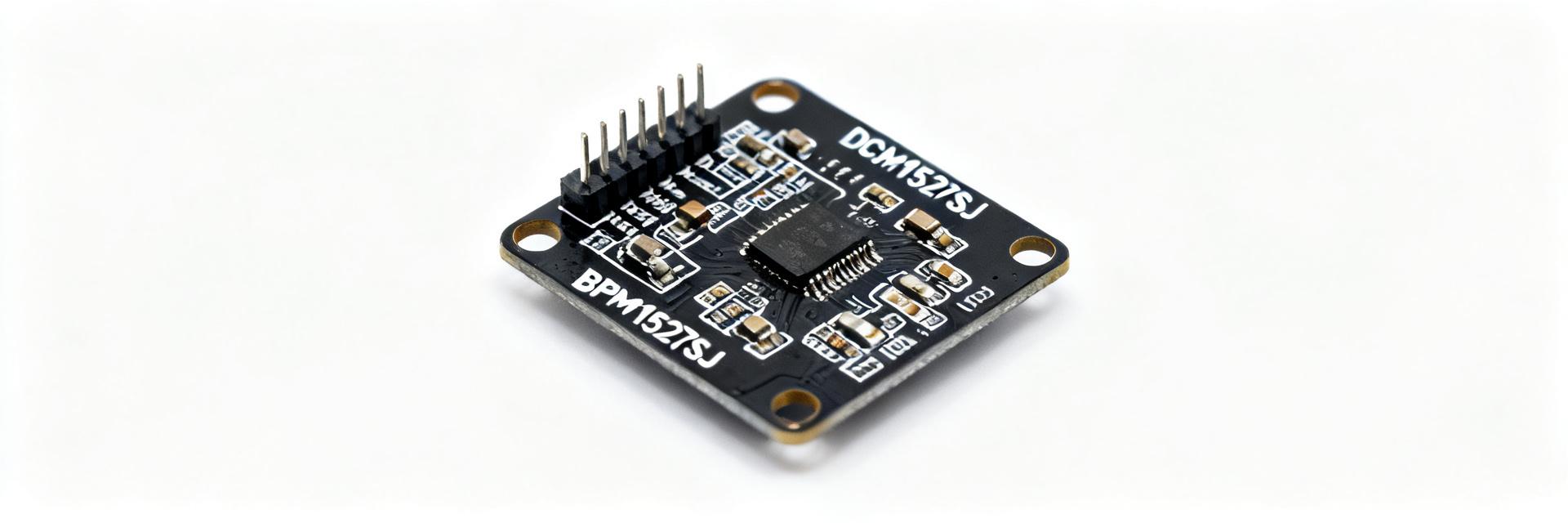
BPM1527SJ Datasheet Deep Dive: Key Specs & Metrics
Modern isolated DC/DC power modules routinely reach high full-load efficiencies and sub-100 mW standby draws. This analysis extracts the BPM1527SJ datasheet essentials to surface key specs for system …
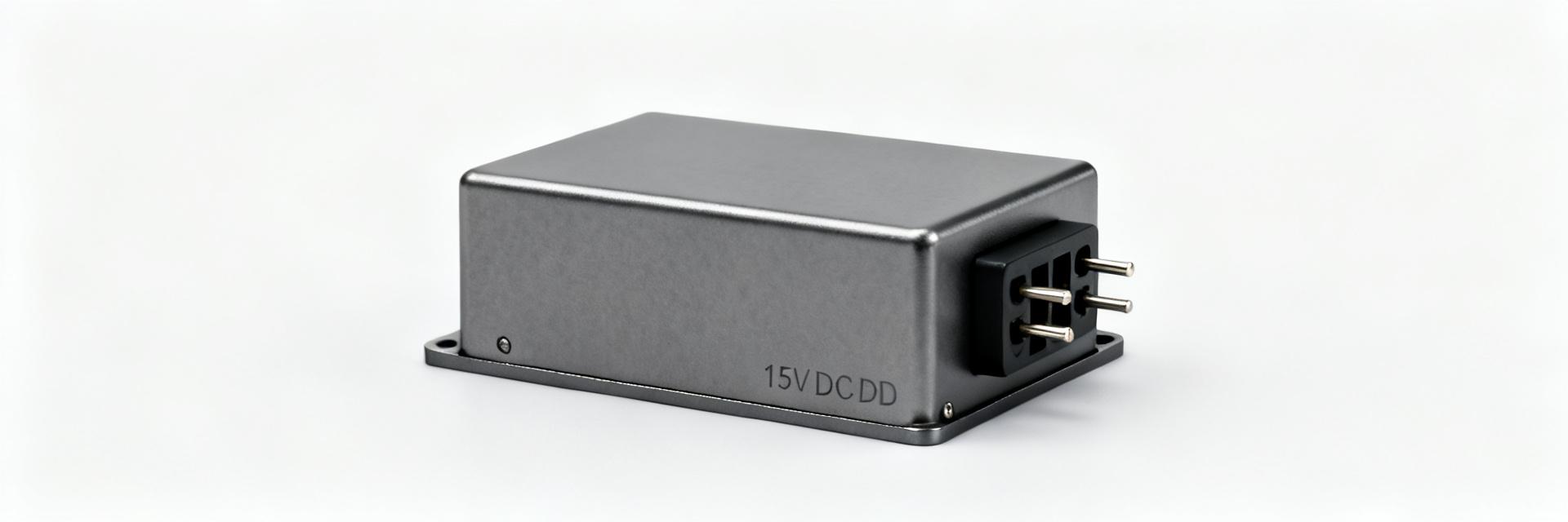
MPM1517SJ Complete Datasheet: Specs, Pinout & Notes
The MPM1517SJ module is a compact DC/DC power module rated for a headline output capability of 15 V at up to 1.7 A continuous from a single package. This module is ideal for regulated rails where boar…
AM29040-50KC Technical Report: Specs, Pinout & Metrics
2026-07-02 10:16:19
STL260N4F7: Detailed Rds(on) Performance Report & Benchmarks
2026-07-02 10:14:23
NTD4815NT4G Complete Specs & Test Data for Engineers
2026-07-02 10:14:20
L07P003D15 datasheet: Full electrical specs & test data
2026-07-02 10:07:24
RGP10M-E3 Diode: Full Specs & Performance Breakdown
2026-07-02 10:05:24
Read more