
The first step in assessing any octal buffer for bus or memory applications is to extract the critical operating points and timing constraints from the manufacturer data. Typical datasheets show a VCC centered near 5V and propagation delays in the low single-digit nanoseconds; these electrical specs determine whether the device can meet your bus timing and drive requirements. This introduction frames the actionable summary and design checklist that follows.
Design Logic
Point: Engineers need a concise map from datasheet tables to board-level decisions.
Evidence: Key tables list VCC range, input thresholds, I/O drive, and timing under specified CL and RL.
Explanation: By focusing on those fields, you can size pull resistors, estimate worst-case path delays, and predict thermal load before committing to prototypes.
Background: What the 74ACT240 Is and Where It’s Used
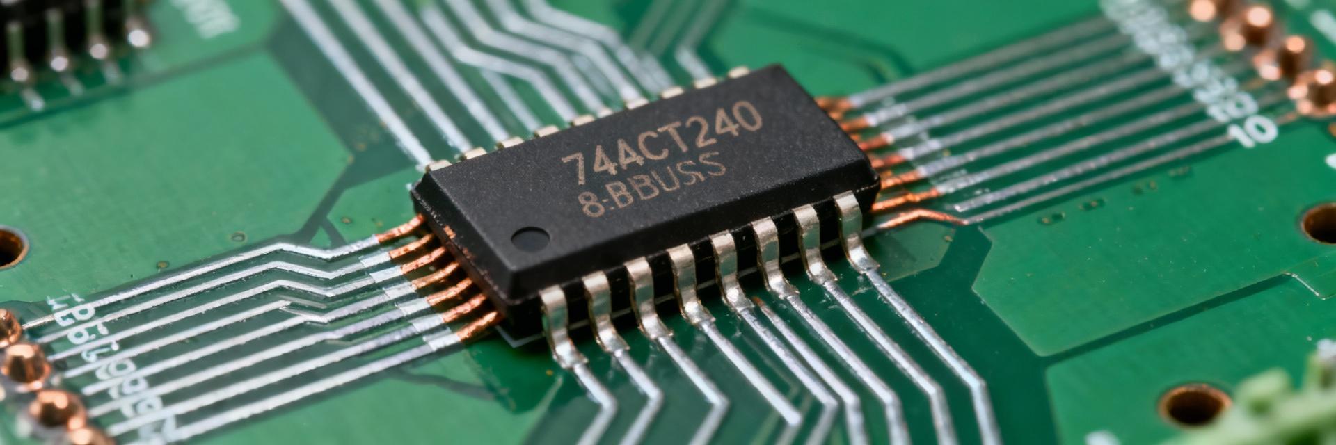
Function Summary — Octal Buffer with 3-State Outputs
Point: This device class is an inverting octal buffer/line driver with tri-state enables used to isolate or drive an 8-bit bus.
Evidence: Typical roles include memory/address drivers, bus transceivers, and clock buffering where inverted signals or controlled bus release are required.
Explanation: Treat it as a parallel driver with two enable halves; unused inputs should be tied to defined logic levels per the datasheet to avoid floating states and excess ICC.
Choosing the 74ACT240 vs. Alternatives
Point: Selection hinges on VCC compatibility, speed, output drive, and power.
Evidence: ACT variants offer TTL-compatible thresholds and low single-digit ns tPD, while AC or HC families trade thresholds and drive for other properties.
Explanation: Choose ACT when TTL thresholds and fast switching are necessary; consider output IOH/IOL and ICC impact for dense, multi-drop bus topologies.
74ACT240 Datasheet: Pinout & Functional Overview
Pin-by-Pin Summary
Point: A concise pin mapping reduces miswiring and speeds PCB layout.
Evidence: Typical pinout maps inputs, outputs, two enable pins, VCC and GND with active-low enables noted.
Explanation: Note required states for unused inputs (tie high/low per datasheet), and document which pins control each 4-bit half when implementing enable sequencing.
Package & Footprint Notes
Point: Package choice affects parasitics and thermal behavior.
Evidence: Common packages include DIP for bench prototyping and SOIC/TSSOP for production with smaller parasitic capacitance in leadless packages.
Explanation: Use DIP or SOIC when prototyping; for high-speed or dense boards prefer small outline packages with careful pad design to limit trace inductance and allow close decoupling.
74ACT240 Datasheet: Electrical Specs & Timing Summary
DC Electrical Analysis
Extract VCC operating range, VIH/VIL, IOH/IOL, ICC and input leakage to size your interface. Use typical figures for behavior and maximums for safety margins.
AC Timing Analysis
Timing depends on specified VCC, CL and RL. Add worst-case tPD for each driver in the path and budget margin for enable/disable to avoid bus contention.
Visualization: Propagation Delay (tPD) Comparison
| Parameter | Typical | Max / Test Condition |
|---|---|---|
| VCC | ~5 V nominal | 4.5V to 5.5V Supply range |
| VIH / VIL | TTL-compatible | 2.0V (High) / 0.8V (Low) |
| IOH / IOL | ±24 mA class | Varies by Temperature |
| tPD | Low single-digit ns | Depends on CL (Typical 50pF) |
Thermal, Absolute Maximum Ratings & Power Considerations
Absolute Maximums
Designing below absolute maximums preserves reliability. Operate with safety margins (e.g., several percent below max VCC), protect against transients, and calculate derating for elevated ambient temperatures to prevent premature failure.
Power & Decoupling
Estimate power from quiescent ICC and switching losses. Power ≈ VCC × ICC + Σ(Cload × VCC2 × f). Place a 0.1 μF decoupling capacitor adjacent to VCC pin and add a 1 μF bulk cap nearby.
Design & Application Guide: Practical Implementation Tips
-
✔
Driving Multi-Drop Buses & Managing 3-State Enables
Proper wiring and enable sequencing prevent contention. Use dedicated enable lines per half, avoid simultaneous enables on multiple drivers, and sequence enables during power-up.
-
✔
Signal Integrity, Level Interfacing & Protection
Fast edges require damping. Add small series resistors (10–33 Ω) at outputs to reduce overshoot. Evaluate level translation if interfacing to non-TTL domains to avoid false switching.
PCB Layout Case Study & Troubleshooting Checklist
Mini Case Study: Layout for an 8-bit Bus Driver
Placement and decoupling determine performance. Place the device adjacent to its primary load, route 8 data traces with matched lengths, and place a 0.1 μF ceramic cap within 1–2 mm of the VCC pin. Keep ground return short and wide.


