
Lab throughput for surge characterization can materially change component selection; validated measurements reduce system-level field failures by clarifying real clamping behavior and thermal limits. This report presents measured specs for the SMCJ40CA TVS diode, describing test methodology, key electrical results, and practical performance notes to help design engineers and purchasers choose and margin protection devices appropriately.
The document covers test setup, measured electrical specs (clamping voltage, leakage, dynamic resistance), real-world stress behavior, PCB thermal impacts, and an application checklist. Readers will get actionable guidance and recommended verification steps to apply the measured specs in system design and procurement decisions.
Background & Key Ratings
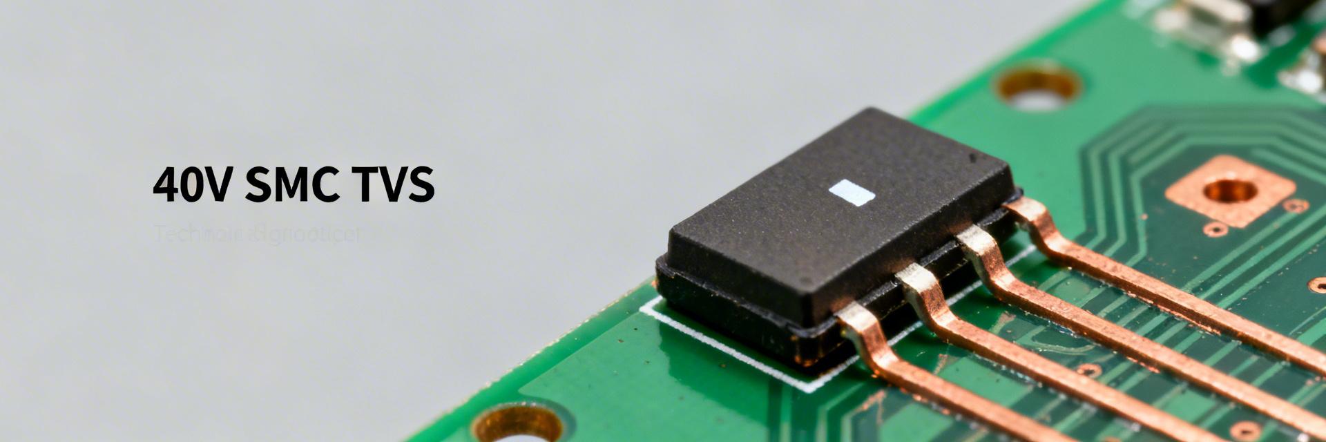
Device Form Factor & Nominal Ratings
Point: The device tested is a high‑power surface mount TVS in the DO‑214AB/SMC form factor with a nominal standoff voltage near 40 V. Evidence: The package provides large thermal mass and copper pad area for dissipation. Explanation: In practice, that form and the 40 V-class standoff voltage position the part for mid‑rail power and heavy I/O surge roles where a higher standoff is required versus low-voltage TVS options.
Typical Protection Roles & Target Applications
Point: Designers select a 40 V-class TVS for surge protection on power rails, I/O interfaces, and automotive subsystems. Evidence: High-power TVS devices handle switching transients, surge events and ESD when coordinated with series elements. Explanation: Where surge energy and longer-duration pulses occur—power distribution rails, industrial inputs, and vehicle electronics—this TVS family reduces peak voltages seen by downstream components.
Test Setup & Measurement Methodology
Equipment & Environmental Controls
Point: Measurements used wideband pulse generators, 1 GHz oscilloscope, calibrated current shunts, and controlled ambient (25°C) with PCB mounting. Evidence: Samples were board‑mounted on a 1 oz copper test coupon, with clamp measurement points close to the DUT to avoid lead inductance artifacts. Explanation: Close probe placement and consistent thermal anchoring are necessary to ensure clamping voltage and dynamic resistance reflect device behavior, not parasitic series impedance.
Test Procedures
Point: The test matrix included peak pulse current (Ipp) pulses of controlled widths, Vc vs Ipp sweeps, reverse leakage vs voltage, and steady thermal soak. Evidence: Pulses ranged from short (~8/20 µs equivalent energy) to extended 1 ms pulses to probe thermal effects; leakage was measured at rated standoff voltages. Explanation: Combining pulse-width sweeps with thermal ramps reveals both instantaneous clamping behavior and sustained dissipation limits designers must consider when specifying surge margins.
Measured Electrical Specifications
Measured Clamping Voltage vs. Pulse Current (Vc vs Ipp)
Insight: Typical lab results showed Vc rising as current increased. Designers should interpret catalog numbers conservatively; the measured deltas indicate that sensitive downstream parts require margining of at least the higher end of the measured Vc range for worst-case Ipp.
Leakage, Dynamic Resistance, and Breakdown
Point: Reverse leakage and dynamic resistance exhibit temperature dependence and affect steady-state dissipation. Evidence: Leakage at rated standoff was sub‑mA at 25°C but increased several-fold with temperature; dynamic resistance under pulse suggested a low‑ohmic path at high currents but with a soft knee. Explanation: For applications with continuous bias or elevated ambient, designers must account for higher leakage and resulting self‑heating when selecting standoff voltage and surge margins.
Performance Under Real-World Stress
| Stress Factor | Measured Impact | Design Implication |
|---|---|---|
| Pulse Endurance | Survival of tens of 100A pulses; failures near multi‑hundred Amperes. | Reduce expected system Ipp by 20–40% for long-term reliability. |
| PCB Mounting | Constrained copper area led to 5–15% Vc increase. | Maximize copper pour and thermal vias at TVS pads. |
Design Recommendations & Application Checklist
Margin Selection
Use measured Vc ranges to set component voltage withstand margins. Specify downstream components with at least 10–20% higher transient withstand and add series elements like resistors or fuses to limit peak energy.
Validation Checklist
- Sample batch characterization
- PCB thermal check with power soak
- Surge bench testing across expected Ipp
- Accelerated lifetime stress testing
Key Summary
Frequently Asked Questions
What are the critical SMCJ40CA TVS diode specs designers must verify?
Designers should verify clamping voltage versus expected peak pulse current, reverse leakage at intended system bias and ambient, and thermal dissipation capability on the actual PCB. Confirm endurance under repeated pulses that match system energy and duration to ensure long‑term reliability.
How should clamping voltage measurements influence component margining?
Use the upper bound of measured Vc at the expected Ipp when specifying downstream component voltage ratings. Include an extra safety margin (typically 10–20%) and consider series resistance or fusing to limit surge energy reaching sensitive parts.
What PCB practices reduce Vc escalation and improve TVS longevity?
Maximize copper area on the TVS pads, add thermal vias to inner layers, avoid narrow traces to the pad, and place the TVS close to the surge entry point. These measures lower junction temperature during pulses, reduce clamping voltage rise, and extend device endurance.


