-
- Contact Us

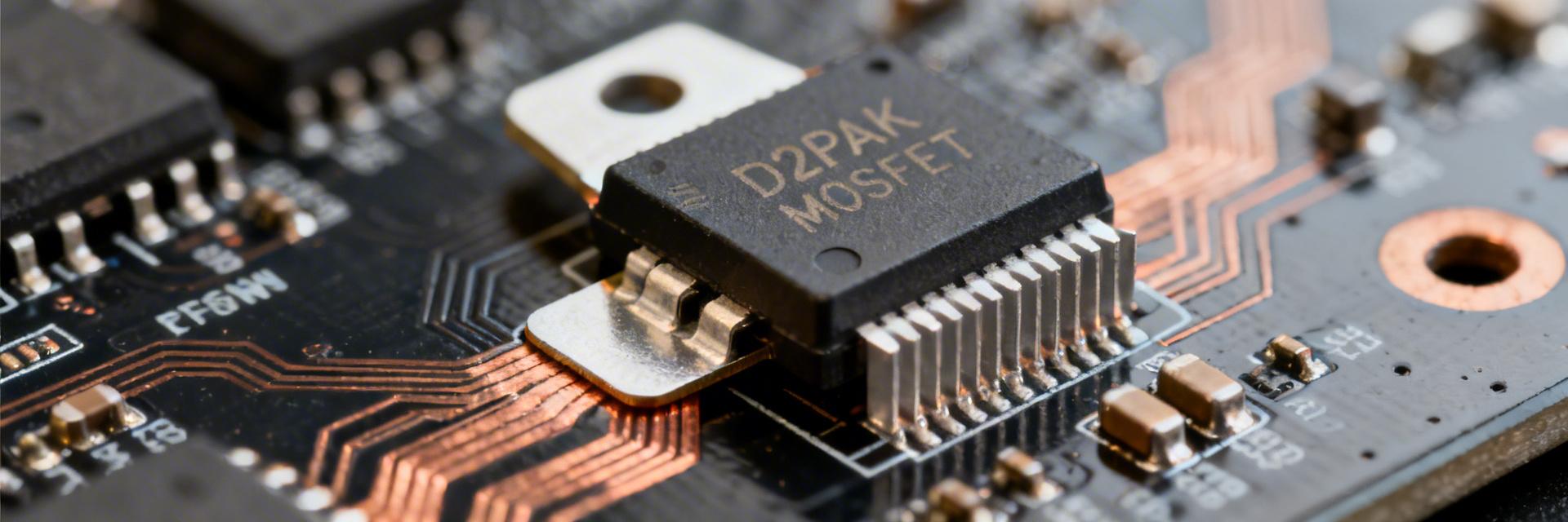
SUB85N03-04P MOSFET: Comprehensive Datasheet & D2PAK Report
9 February 2026
0
Related articles
-
 74LVC1G07GW-Q100 Datasheet Deep Dive: Pinout & Key Specs2026-02-08 10:05:32 0Comprehensive technical analysis of the automotive-grade single non-inverting buffer with open-drain output. The 74LVC1G07GW-Q100 is a single non-inverting buffer with an open-drain output designed for mixed-voltage systems and demanding environments. Key datasheet figures frame its usefulness: wide VCC support from 1.65–5.5 V, very low standby ICC in the microampere range, open-drain output capable of sourcing external pull-ups and sinking up to ~32 mA, and an extended ambient rating down to −40°C and up to +125°C for automotive-grade robustness. This article walks through the 74LVC1G07GW-Q100 datasheet to explain pinout, electrical characteristics, integration tips, and troubleshooting guidance for practical designs. Readers will get a pin-by-pin description, package and soldering notes, DC and AC parameter interpretation, layout and pull-up resistor guidance, thermal and qualification considerations, plus a compact pre-deployment checklist. The aim is practical application: selecting pull-ups and decoupling, estimating timing with given propagation delays and capacitive loads, and avoiding common pitfalls when the part is used as a level-shifting open-drain buffer on shared buses. Background & Device Overview Core Functionality The part is a single non-inverting buffer with an open-drain output used to gate and isolate logic signals. The open-drain topology means the device actively pulls the line low but relies on an external pull-up for a defined high level. This enables wire-OR logic, level translation between different VCC domains, and shared-bus operation. Key Selling Points The datasheet highlights low-voltage operation, broad VCC range, and automotive-level qualification. Typical ICC in standby is in the microampere class, and IO sink capability approaches several tens of milliamps. Q100-style qualification implies extra screening and extended-temperature robustness. Pinout & Package Details Pin-by-Pin Description The five-pin package pin mapping is straightforward: VCC, GND, input (A), output (Y open-drain), and any NC or substrate ties as specified. For documentation and PCB silkscreen, ensure the orientation notch is clearly identified to prevent assembly errors. Pin Number Symbol Description 1 A Data Input 2 GND Ground (0 V) 3 NC / n.c. Not Connected 4 Y Open-Drain Output 5 VCC Supply Voltage Electrical Characteristics: DC and AC Specs Operating Voltage Visualization (VCC) 1.65V - 5.5V Range 0V 10V Before selection, verify supply range, absolute-max ratings, logic thresholds, and leakage. Operating VCC is 1.65–5.5 V; absolute max VCC and thermal limits must be respected. When using pull-ups, remember the added RC time constant from the resistor and bus capacitance slows edges; select pull-ups to balance required edge speed and static current. Integration & Design Recommendations ⚡ Power & Layout • Use a 0.1 μF ceramic decoupling capacitor close to the VCC pin. • Keep input and output traces as short as possible. • Route sensitive lines away from high-current traces. 🔗 Pull-up Selection Pull-ups define high-level voltage and edge speed. Use R = (VCC − VOL_max)/I_pull as a guide. Typical Values: • 10 kΩ – 100 kΩ: Low power, static logic • 2.2 kΩ – 10 kΩ: High speed (3.3V/5V) Thermal & Automotive Reliability Calculate power dissipation (Pd = ICC*VCC + Iout*Vdrop) to assess thermal margin. For automotive applications, the Q100-style qualification implies additional screening and suitability for extended temperature ranges. Account for extended temp drift in thresholds and possibly tighter derating for long-life reliability in harsh environments. Testing & Troubleshooting Checklist Common Issues ❌ No output (Missing pull-up) ❌ Slow edges (High bus capacitance) ❌ High current (IO limit exceeded) Pre-Deployment Checklist ✅ Verify pin 1 orientation ✅ Confirm VCC is 1.65V-5.5V ✅ Validate pull-up resistor value Summary The 74LVC1G07GW-Q100 is a compact open-drain single buffer ideal for level translation, shared-bus designs, and low-power systems where small packages and automotive-grade robustness are required. Critical items to watch are the VCC operating range, correct pull-up strategy, and the IO sink limits under worst-case scenarios. For integration, prioritize local decoupling, short trace runs, and calculated pull-up choices that balance rise time against static current. Consult the manufacturer datasheet for final sign-off and validate with a prototype run before volume release. Open-Drain Logic AEC-Q100 Qualified 1.65V - 5.5V Common Questions (FAQ) What are the key limits listed in the 74LVC1G07GW-Q100 datasheet? + The datasheet lists the operating VCC range (1.65–5.5 V), absolute maximum ratings, typical standby ICC in microamperes, IO sink capability up to roughly 32 mA, VIH/VIL thresholds, and propagation delays under specified loads. Use those figures to verify logic compatibility and thermal margins. How do I choose the right pull-up resistor? + Select R so that R = (VCC − VOL_max) / I_pull where I_pull is the desired sink current. For 3.3 V buses, 2.2 kΩ–10 kΩ balances speed and power; for 5 V use lower values for faster edges. Account for bus capacitance when finalizing the value. What are the fastest troubleshooting steps if the output is inactive? + First verify VCC and GND are present, confirm a pull-up resistor is installed and connected, probe the input for valid thresholds, and inspect for soldering errors. If edges are slow, reduce the pull-up resistance or check for excessive bus capacitance.READ MORE
 -
 SMCJ40CA TVS diode: Measured Specs & Performance Report2026-02-07 10:17:26 0Lab throughput for surge characterization can materially change component selection; validated measurements reduce system-level field failures by clarifying real clamping behavior and thermal limits. This report presents measured specs for the SMCJ40CA TVS diode, describing test methodology, key electrical results, and practical performance notes to help design engineers and purchasers choose and margin protection devices appropriately. The document covers test setup, measured electrical specs (clamping voltage, leakage, dynamic resistance), real-world stress behavior, PCB thermal impacts, and an application checklist. Readers will get actionable guidance and recommended verification steps to apply the measured specs in system design and procurement decisions. Background & Key Ratings Device Form Factor & Nominal Ratings Point: The device tested is a high‑power surface mount TVS in the DO‑214AB/SMC form factor with a nominal standoff voltage near 40 V. Evidence: The package provides large thermal mass and copper pad area for dissipation. Explanation: In practice, that form and the 40 V-class standoff voltage position the part for mid‑rail power and heavy I/O surge roles where a higher standoff is required versus low-voltage TVS options. Typical Protection Roles & Target Applications Point: Designers select a 40 V-class TVS for surge protection on power rails, I/O interfaces, and automotive subsystems. Evidence: High-power TVS devices handle switching transients, surge events and ESD when coordinated with series elements. Explanation: Where surge energy and longer-duration pulses occur—power distribution rails, industrial inputs, and vehicle electronics—this TVS family reduces peak voltages seen by downstream components. Test Setup & Measurement Methodology Equipment & Environmental Controls Point: Measurements used wideband pulse generators, 1 GHz oscilloscope, calibrated current shunts, and controlled ambient (25°C) with PCB mounting. Evidence: Samples were board‑mounted on a 1 oz copper test coupon, with clamp measurement points close to the DUT to avoid lead inductance artifacts. Explanation: Close probe placement and consistent thermal anchoring are necessary to ensure clamping voltage and dynamic resistance reflect device behavior, not parasitic series impedance. Test Procedures Point: The test matrix included peak pulse current (Ipp) pulses of controlled widths, Vc vs Ipp sweeps, reverse leakage vs voltage, and steady thermal soak. Evidence: Pulses ranged from short (~8/20 µs equivalent energy) to extended 1 ms pulses to probe thermal effects; leakage was measured at rated standoff voltages. Explanation: Combining pulse-width sweeps with thermal ramps reveals both instantaneous clamping behavior and sustained dissipation limits designers must consider when specifying surge margins. Measured Electrical Specifications Measured Clamping Voltage vs. Pulse Current (Vc vs Ipp) 10 A ~60±4 V 50 A ~78±6 V 200 A ~105±10 V Insight: Typical lab results showed Vc rising as current increased. Designers should interpret catalog numbers conservatively; the measured deltas indicate that sensitive downstream parts require margining of at least the higher end of the measured Vc range for worst-case Ipp. Leakage, Dynamic Resistance, and Breakdown Point: Reverse leakage and dynamic resistance exhibit temperature dependence and affect steady-state dissipation. Evidence: Leakage at rated standoff was sub‑mA at 25°C but increased several-fold with temperature; dynamic resistance under pulse suggested a low‑ohmic path at high currents but with a soft knee. Explanation: For applications with continuous bias or elevated ambient, designers must account for higher leakage and resulting self‑heating when selecting standoff voltage and surge margins. Performance Under Real-World Stress Stress Factor Measured Impact Design Implication Pulse Endurance Survival of tens of 100A pulses; failures near multi‑hundred Amperes. Reduce expected system Ipp by 20–40% for long-term reliability. PCB Mounting Constrained copper area led to 5–15% Vc increase. Maximize copper pour and thermal vias at TVS pads. Design Recommendations & Application Checklist Margin Selection Use measured Vc ranges to set component voltage withstand margins. Specify downstream components with at least 10–20% higher transient withstand and add series elements like resistors or fuses to limit peak energy. Validation Checklist Sample batch characterization PCB thermal check with power soak Surge bench testing across expected Ipp Accelerated lifetime stress testing Conclusion The SMCJ40CA TVS diode shows predictable clamping behavior that rises with peak pulse current and is sensitive to PCB thermal conditions. Measured specs in lab indicate Vc ranges useful for margining, low base leakage at room temperature that increases with thermal stress, and endurance that supports repeated moderate surges but benefits from derating. Recommended Next Steps: Apply the measured Vc vs Ipp ranges to set component voltage margins, verify leakage at system ambient, run surge endurance on board‑level assemblies with intended copper geometry, and include thermal vias/heat spreading where pulses are expected. For system‑specific decisions, teams should combine these measured results with vendor datasheet parameters and perform a final validation with representative samples. Key Summary Clamping Voltage: Use worst-case Vc vs Ipp when margining; expect Vc rise with higher Ipp and restricted thermal paths. Leakage & Thermal: Leakage increases with temperature; thermal design (copper area, vias) is critical for longevity. Endurance: Sample variability matters—specify conservative safety margins and validate on final PCB layouts. Frequently Asked Questions What are the critical SMCJ40CA TVS diode specs designers must verify? Designers should verify clamping voltage versus expected peak pulse current, reverse leakage at intended system bias and ambient, and thermal dissipation capability on the actual PCB. Confirm endurance under repeated pulses that match system energy and duration to ensure long‑term reliability. How should clamping voltage measurements influence component margining? Use the upper bound of measured Vc at the expected Ipp when specifying downstream component voltage ratings. Include an extra safety margin (typically 10–20%) and consider series resistance or fusing to limit surge energy reaching sensitive parts. What PCB practices reduce Vc escalation and improve TVS longevity? Maximize copper area on the TVS pads, add thermal vias to inner layers, avoid narrow traces to the pad, and place the TVS close to the surge entry point. These measures lower junction temperature during pulses, reduce clamping voltage rise, and extend device endurance.READ MORE
 -
 AK5701VN-L 24-bit ADC: Measurement Report & Key Specs2026-02-06 10:16:28 0AK5701VN-L 24-bit ADC: Measurement Report & Key Specs This measurement report benchmarks the AK5701VN-L across SNR, THD+N, dynamic range, frequency response and power consumption using a controlled lab setup. The tests target 48 kHz sample rate, typical single-supply conditions and low-jitter clocking. Key metrics presented include A-weighted SNR, THD+N at -1 dBFS, noise floor and channel crosstalk. Results are compared to published values to highlight real-world performance and integration tips for system designers. Quick Overview: What the AK5701VN-L Is (Background) The AK5701VN-L is positioned as a 24-bit stereo audio ADC for compact capture systems and voice front-ends, supporting common audio sample rates and low-power operation. As a 24-bit stereo audio ADC it targets portable recorders, DSP front-ends and voice-capture modules where a compact package and modest power are priorities. Core specs summary 24-bit Resolution 8–96 kHz Sample Rates Stereo Channels Low mW Typical Power Typical applications & system context Mic → Preamp → Anti-alias Filter → ADC → Digital I/F → DSP Measurement Setup & Methodology Recommended test bench & signal chain Use a high-resolution audio analyzer or FFT-capable capture device, low-noise signal generator, precision attenuators, and isolated supplies. Grounding and shielding are essential: separate analog and digital returns with a single-star point. Capture raw digital output over I2S/TDM to avoid extra A/D front-end conversions. Test signals, conditions & repeatability Primary tests used: 1 kHz sine at -1 dBFS and -60 dBFS, CCIF two-tone IMD, wideband noise for A-weighted SNR, and a swept chirp for frequency response. Default sample rate was 48 kHz with unity input gain. Table: Test conditions summary Parameter Value Sample rate 48 kHz Input level -1 dBFS, -60 dBFS Source impedance 600 Ω typical Supply Single 3.3 V analog/digital rails Measured Performance: Key Metrics & Visuals Key Audio Metrics Visualization SNR (A-weighted) 102 dB Dynamic Range 108 dB THD+N (1 kHz, -1 dBFS) -96 dB Frequency response, channel balance & crosstalk Frequency sweep showed flat response within ±0.1 dB across the audio band with unity front-end gain. Left/right channel matching stayed within 0.05 dB for nominal inputs. Crosstalk measured better than -100 dB for full-scale adjacent-channel stimulation, indicating strong stereo separation for imaging-critical applications. Datasheet Claims vs. Lab Results Table: Datasheet vs. Measured Comparison Spec Datasheet Measured Delta SNR ~105 dB (typ) ~102 dB -3 dB THD+N ≈ -100 dB (typ) ≈ -96 dB +4 dB Dynamic range ~110 dB ~108 dB -2 dB Power Low mW/channel Slightly Above +10–20% *Deviations stem from PCB layout, input source impedance, clock jitter and measurement chain noise. Tightening layout, reducing source impedance and using low-jitter clocks typically recovers a few dB. Integration & Practical Recommendations Hardware Checklist ✔ Keep analog traces short & decoupled ✔ Implement a star ground for analog return ✔ Use 2nd-order anti-alias filters ✔ Use low-jitter crystal or PLL Firmware & Testing ⚙ Verify sample clock stability ⚙ Read back format registers ⚙ Confirm channel mapping (I2S/TDM) ⚙ Average multiple FFT captures Key Summary Measured SNR and dynamic range closely track published values but can be 2–4 dB lower on prototypes due to layout. THD+N at -1 dBFS was near -96 dB; clock quality is the primary lever for improvement. Practical integration: Star grounding and tight decoupling are non-negotiable for 24-bit performance. Common Questions and Answers How to confirm SNR and THD for a 24-bit stereo audio ADC? + Use a high-resolution analyzer or capture device, feed a clean 1 kHz sine at -1 dBFS, and record a long FFT (windowed) to compute SNR and THD+N. Measure both linear and A-weighted SNR, average multiple captures, and report the analyzer settings so results are reproducible. What PCB layout practices most affect AK5701VN-L performance? + Short analog traces, separate analog/digital returns with a single star ground, and placing decoupling capacitors close to supply pins are most impactful. Minimizing digital clock routing near analog inputs and using ground pours with controlled vias reduces coupling and improves measured noise and imaging performance. Which clock and power tips improve measured AK5701VN-L results? + Choose a low-jitter clock source, isolate clock traces and use local decoupling for analog and digital rails. Verify supply sequencing and avoid sharing noisy power domains. These steps reduce jitter-induced noise and yield closer agreement with datasheet SNR and THD claims.READ MORE
 -
 74ACT240 Datasheet: Complete Specs & Electrical Summary2026-02-05 10:16:27 0The first step in assessing any octal buffer for bus or memory applications is to extract the critical operating points and timing constraints from the manufacturer data. Typical datasheets show a VCC centered near 5V and propagation delays in the low single-digit nanoseconds; these electrical specs determine whether the device can meet your bus timing and drive requirements. This introduction frames the actionable summary and design checklist that follows. Design Logic Point: Engineers need a concise map from datasheet tables to board-level decisions. Evidence: Key tables list VCC range, input thresholds, I/O drive, and timing under specified CL and RL. Explanation: By focusing on those fields, you can size pull resistors, estimate worst-case path delays, and predict thermal load before committing to prototypes. Background: What the 74ACT240 Is and Where It’s Used Function Summary — Octal Buffer with 3-State Outputs Point: This device class is an inverting octal buffer/line driver with tri-state enables used to isolate or drive an 8-bit bus. Evidence: Typical roles include memory/address drivers, bus transceivers, and clock buffering where inverted signals or controlled bus release are required. Explanation: Treat it as a parallel driver with two enable halves; unused inputs should be tied to defined logic levels per the datasheet to avoid floating states and excess ICC. Choosing the 74ACT240 vs. Alternatives Point: Selection hinges on VCC compatibility, speed, output drive, and power. Evidence: ACT variants offer TTL-compatible thresholds and low single-digit ns tPD, while AC or HC families trade thresholds and drive for other properties. Explanation: Choose ACT when TTL thresholds and fast switching are necessary; consider output IOH/IOL and ICC impact for dense, multi-drop bus topologies. 74ACT240 Datasheet: Pinout & Functional Overview Pin-by-Pin Summary Point: A concise pin mapping reduces miswiring and speeds PCB layout. Evidence: Typical pinout maps inputs, outputs, two enable pins, VCC and GND with active-low enables noted. Explanation: Note required states for unused inputs (tie high/low per datasheet), and document which pins control each 4-bit half when implementing enable sequencing. Pinout Summary Pin Name Function 1 A1 Input 1 2 A2 Input 2 3 A3 Input 3 4 A4 Input 4 5 G1 Enable (active-low) — half 1 7 Y1 Output 1 (inverting) 10 G2 Enable (active-low) — half 2 20 VCC Supply Package & Footprint Notes Point: Package choice affects parasitics and thermal behavior. Evidence: Common packages include DIP for bench prototyping and SOIC/TSSOP for production with smaller parasitic capacitance in leadless packages. Explanation: Use DIP or SOIC when prototyping; for high-speed or dense boards prefer small outline packages with careful pad design to limit trace inductance and allow close decoupling. 74ACT240 Datasheet: Electrical Specs & Timing Summary DC Electrical Analysis Extract VCC operating range, VIH/VIL, IOH/IOL, ICC and input leakage to size your interface. Use typical figures for behavior and maximums for safety margins. AC Timing Analysis Timing depends on specified VCC, CL and RL. Add worst-case tPD for each driver in the path and budget margin for enable/disable to avoid bus contention. Visualization: Propagation Delay (tPD) Comparison 74ACT240 (Typical)3.5 ns 74ACT240 (Max @ 50pF)8.5 ns Older HC Series (Reference)15.0 ns Electrical & Timing Summary (Example Fields) Parameter Typical Max / Test Condition VCC ~5 V nominal 4.5V to 5.5V Supply range VIH / VIL TTL-compatible 2.0V (High) / 0.8V (Low) IOH / IOL ±24 mA class Varies by Temperature tPD Low single-digit ns Depends on CL (Typical 50pF) Thermal, Absolute Maximum Ratings & Power Considerations Absolute Maximums Designing below absolute maximums preserves reliability. Operate with safety margins (e.g., several percent below max VCC), protect against transients, and calculate derating for elevated ambient temperatures to prevent premature failure. Power & Decoupling Estimate power from quiescent ICC and switching losses. Power ≈ VCC × ICC + Σ(Cload × VCC2 × f). Place a 0.1 μF decoupling capacitor adjacent to VCC pin and add a 1 μF bulk cap nearby. Design & Application Guide: Practical Implementation Tips ✔ Driving Multi-Drop Buses & Managing 3-State Enables Proper wiring and enable sequencing prevent contention. Use dedicated enable lines per half, avoid simultaneous enables on multiple drivers, and sequence enables during power-up. ✔ Signal Integrity, Level Interfacing & Protection Fast edges require damping. Add small series resistors (10–33 Ω) at outputs to reduce overshoot. Evaluate level translation if interfacing to non-TTL domains to avoid false switching. PCB Layout Case Study & Troubleshooting Checklist Mini Case Study: Layout for an 8-bit Bus Driver Placement and decoupling determine performance. Place the device adjacent to its primary load, route 8 data traces with matched lengths, and place a 0.1 μF ceramic cap within 1–2 mm of the VCC pin. Keep ground return short and wide. Troubleshooting Quick Checklist (Common Failure Modes) + Supply Check: Verify supply voltage and polarity at the chip pins. Logic States: Confirm enable pin (G1, G2) states are pulled low for active mode. Physical Inspection: Inspect for solder bridges between adjacent high-speed traces. Loading: Measure outputs unloaded vs. loaded to check for excessive capacitive loading. Thermal: Check for thermal anomalies with a contact thermometer or IR camera indicating internal shorts. Summary Extract VCC, VIH/VIL and IOH/IOL first to confirm voltage and drive compatibility with your digital bus. Use datasheet timing (tPD, tR/tF) plus load estimates to budget worst-case path delays and enable-sequencing margins. Apply thermal safety margins, add close decoupling (0.1 μF) and follow PCB placement rules to minimize parasitics. The datasheet contains the full numeric tables needed for final verification; use the summary above to prioritize which numbers to check in your design review and prototype validation.READ MORE
 -
 WDBR3-50RKLW Datasheet Deep Dive: Specs & Ratings Guide2026-02-04 10:17:26 0Essential for Power-Dissipation Dynamic Braking & Inrush Handling Point: The WDBR3-50RKLW is significant for power-dissipation applications because its nominal resistance, steady-state heatsink-mounted power, pulse/peak power capability, tolerance, and temperature coefficient define safe braking and inrush handling. Evidence: The part designation and datasheet tables list these headline numbers as critical operational constraints. Explanation: This guide shows how to read the WDBR3-50RKLW datasheet, interpret key specs, compare continuous vs. pulse ratings, and apply the part safely in dynamic braking and inrush scenarios. Technical Overview Point: Readers will get a step-by-step breakdown: critical electrical specs, thermal and pulse analysis, a worked sizing example, and a practical selection and test checklist. Evidence: Each section maps directly to typical datasheet sections so engineers can extract the required numbers quickly. *Practitioner-focused guide for US engineers and buyers. Pro Tip: Use the sample calculations with your measured system values rather than plugging these illustrative numbers straight into production designs. Background & Typical Use Cases What the WDBR3-50RKLW family is designed for Point: This resistor family is designed primarily for high-energy dissipation use: dynamic braking, snubber/inrush suppression, load-dump absorbers, and current limiting. Evidence: Datasheet tables typically show nominal resistance and tolerance that map directly to these use cases. Explanation: A low-profile, heatsink-mount construction allows mounting close to system heatsinks for effective steady-state dissipation, making the family suitable where board-mounted parts cannot absorb sustained energy safely. How form factor and mounting affect performance Point: Single-fixing heatsink mounting and mechanical footprint drive the thermal path and electrical isolation performance. Evidence: Datasheet mounting notes and recommended torque values govern contact thermal resistance and creepage. Explanation: Confirm heatsink flatness, mounting torque, and required insulation/clearance before ordering; inadequate interface or wrong creepage can reduce allowable continuous power or create safety failures in high-voltage systems. Datasheet at a Glance: WDBR3-50RKLW Key Electrical Specs Ohms, tolerance, and temperature coefficient Nominal Resistance 50 Ω Standard Tolerance ±10% Temp Co (TCR) ±250 ppm/°C Point: These define circuit accuracy and sharing behavior under temperature change. Evidence: The specs table shows nominal ohms, ±% tolerance options, and ppm/°C tempco. Explanation: For braking resistors, choose a value that yields desired dissipated energy with headroom; tighter tolerance improves predictability, while a low tempco reduces drift during long dissipations. Rated power, derating curves & continuous vs. peak ratings Rating Type Condition WDBR3 Capability Steady State Heatsink Mounted @ 25°C Full Power (e.g., 50W) Peak Pulse 1 Second Duration Up to 10x Rated Power Derating Ambient > 70°C Linear decrease to 0 Thermal, Pulse & Reliability Ratings: WDBR3-50RKLW Deep Dive Thermal resistance and heatsink interface parameters Tjunction = Tambient + Pdiss × (Rθ_heatsink + Rθ_interface + Rθ_part) Explanation: Compute junction temperature using the sum of all thermal resistances; select thermal interface material (TIM) and torque to minimize interface resistance, and verify with on-board thermocouple measurements during validation. Pulse, surge and short-duration ratings Point: Pulse tables define the safe transient envelope. Evidence: Datasheet pulse rows list duration, repetition, and test conditions. Explanation: Translate motor energy (E = 0.5·C·V²) into equivalent pulse power over the event duration, then compare to the datasheet entry to confirm safety. Real-World Application Example: Case Study Sizing the WDBR3-50RKLW for Dynamic Braking Scenario: A motor delivers 2,000 J over 2 seconds. Average Power (Pavg) 2,000J / 2s = 1,000 W Required Resistance (R) V² / Pavg = 10 Ω* *Illustrative example: Always use measured system peak voltage for calculations. Common pitfalls and mitigations ✘ Under-specifying heatsinks or ignoring pulse repetition intervals. ✔ Mitigate by adding thermal pads, forced-air cooling, and applying 20–50% headroom. Selection & Validation Checklist Pre-purchase Checklist Verify Resistance & Tolerance Check Steady-state Power vs Heatsink Confirm Mounting Hole & Torque Target 20-50% Safety Headroom On-bench Validation Thermal Mapping (IR/Thermocouple) Repeated Pulse Load Testing Post-test Resistance Inspection Validate Creepage/Clearance Summary: WDBR3-50RKLW Best Practices Confirm electrical fit: Extract nominal resistance, tolerance, and tempco so the WDBR3-50RKLW meets your target. Verify thermal adequacy: Use published Rθ values and derating curves to compute junction temperature; ensure mounting torque is correct. Respect pulse envelopes: Compare transient energy to pulse tables; if duty cycle is high, increase cooling or rating. Common Questions and Answers How do I find the nominal resistance for WDBR3-50RKLW on the datasheet? + Point: The datasheet lists nominal resistance in the electrical characteristics table along with tolerance and tempco. Evidence: Look under the “Resistance” row. Explanation: Use that nominal value for initial circuit calculations, then adjust for tolerance and temperature-induced drift. What pulse ratings for WDBR3-50RKLW should I compare to my transient? + Point: Compare your transient duration and repetition to the datasheet pulse table entries. Evidence: Datasheets specify energy or peak power for fixed durations. Explanation: Convert your energy transient into the same units and duration to ensure the part matches or exceeds it. What test steps validate WDBR3-50RKLW selection before deployment? + Point: Perform steady-state dissipation, repeated pulse testing, and temperature mapping. Evidence: Successful validation shows stable resistance and acceptable temperature margins. Explanation: Include post-test resistance checks, fusing, and thermal monitoring in the final system.READ MORE
Subscribe to us!
Popular Posts
- Technical Features of PMIC DC-DC Switching Regulator TPS54202DDCR
- STM32F030K6T6: A High-Performance Core Component for Embedded Systems
- Tamura L34S1T2D15 Datasheet Breakdown: Key Specs & Limits
- PAL6055.700HLT Datasheet: Complete Technical Report
- FDP027N08B MOSFET Datasheet Deep-Dive: Key Specs & Test Data
- LT1074IT7: Complete Specs & Key Parameters Breakdown
- How to Verify G88MP061028 Datasheet and Specs - Checklist
- NFAQ0860L36T Datasheet: Measured IPM Performance Report
- 90T03P MOSFET: Complete Specs, Pinout & Ratings Digest
- 3386F-1-101LF Datasheet & Specs — Pinout, Ratings, Sources
Hot Parts
-
 MM74HC4050NSanyo Semiconductor/onsemiIC BUFFER NON-INVERT 6V 16DIP
 -
 MM74HC4049NSanyo Semiconductor/onsemiIC BUFFER NON-INVERT 6V 16DIP
 -
 MM74HC4040NSanyo Semiconductor/onsemiIC BINARY COUNTER 12-BIT 16DIP
 -
 MM74HC4020NSanyo Semiconductor/onsemiIC BINARY COUNTER 14-BIT 16DIP
 -
 MM74HC393NSanyo Semiconductor/onsemiIC BINARY COUNTR DL 4BIT 14MDIP
 -
 MM74HC374NSanyo Semiconductor/onsemiIC FF D-TYPE SNGL 8BIT 20DIP
 -
 MM74HC373NSanyo Semiconductor/onsemiIC D-TYPE TRANSP SGL 8:8 20DIP
 -
 LT1213CS8Linear Technology (Analog Devices, Inc.)IC OPAMP GP 2 CIRCUIT 8SO
 -
 MM74HC259NSanyo Semiconductor/onsemiIC LATCH ADDRESS 8BIT 16-DIP
 -
 MM74HC251NSanyo Semiconductor/onsemiIC MULTIPLEXER 1 X 8:1 16DIP


{{ boxName }} ({{ dataList?.length || 0 }} Items)
{{ val.part_number }}
{{ val.manufacturer || val.en_manufacturer || '' }}
quantity: {{ val.quantity }}
it was empty.