-
- Contact Us

G9131-25T73UF Datasheet: Pinout & Electrical Ratings
Recent board-level surveys and power-budget benchmarks show designers increasingly prioritize low-dropout regulators with clear pinouts and conservative electrical ratings to avoid field failures. This practical breakdown references the G9131-25T73UF datasheet to give an author-ready, bench-focused summary of pin assignments, operating limits, and the design actions engineers need to prevent margin loss and thermal issues.
The following sections translate datasheet language into actionable design checks: which pins require capacitors, which electrical ratings are guaranteed versus typical, and the PCB/thermal measures needed to meet long-term reliability. Each H2/H3 follows a point → datasheet-evidence → explanation pattern so readers can map measurements directly back to layout and test steps.
(1/5) Overview: What the G9131-25T73UF Is and Where to Use It
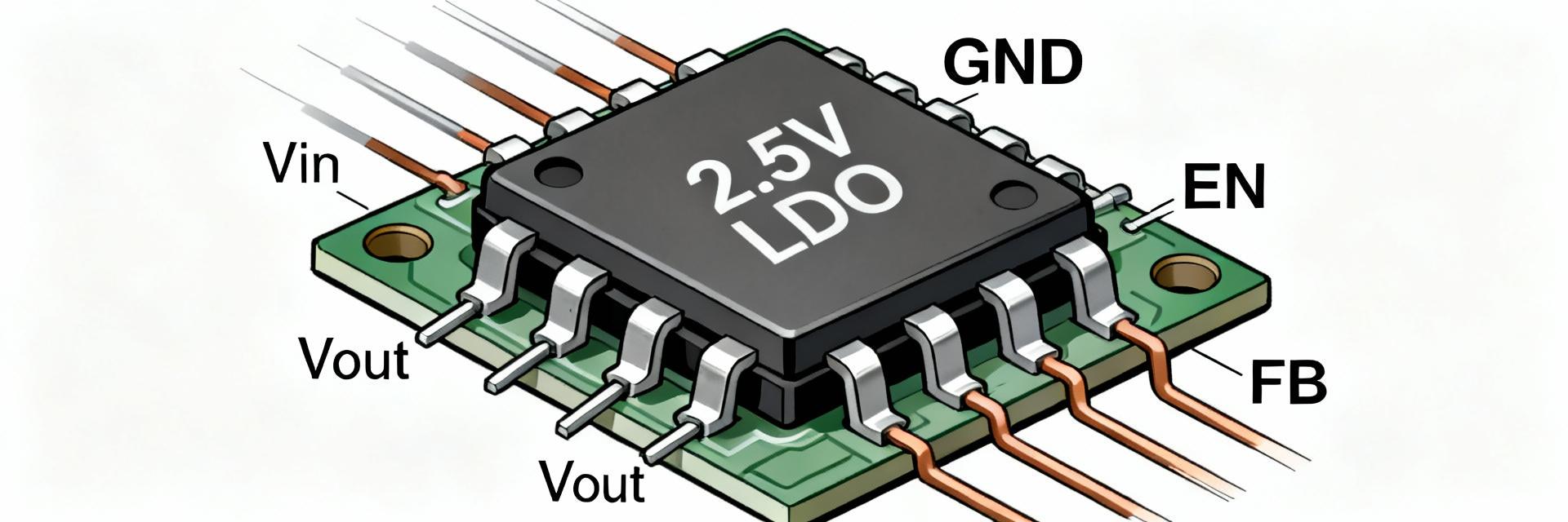
The G9131-25T73UF is a fixed-output low-dropout (LDO) linear regulator optimized for low-noise, battery-powered and sensor-node rails. From the datasheet values, the part provides a 2.5V output (fixed), low quiescent current for standby, and a typical dropout in the sub-500 mV range under light-to-moderate load. Use this part where stable reference rails or low-noise analog supplies are required and where thermal dissipation can be managed on the PCB.
Key features at a glance
- Output voltage: 2.5 V (fixed) — datasheet value; verify tolerance and trim options in the full spec.
- Typical dropout: ~300–400 mV at moderate load (datasheet typical) — confirm guaranteed dropout in worst-case tables.
- Quiescent current: low-µA to 100s of µA class (datasheet typical) — important for battery life budgeting.
- Package family: small SMD with exposed thermal pad — check mechanical drawing for land pattern.
Typical applications & selection criteria
Point: apply the G9131-25T73UF in battery-powered devices, sensor nodes, and precision analog rails. Evidence: its low quiescent current and modest dropout make it suitable where standby efficiency and headroom are constrained. Explanation: choose this regulator when the system requires a fixed 2.5V rail with good transient response; evaluate tradeoffs vs. alternatives on noise, dropout, and thermal headroom before committing to layout.
(2/5) Electrical Ratings & Absolute Maximums from the G9131-25T73UF Datasheet
Electrical ratings define safe operating envelopes and test boundaries. Designers must review recommended VIN range, guaranteed VOUT tolerance, dropout under specified load, and absolute maximum conditions to set margin. Below are compact datasheet-derived numbers for quick reference; always verify against the official electrical ratings table when finalizing supplier selection.
Operating ranges: VIN, VOUT, dropout and tolerance
Point: recommended input and output ranges and dropout behavior determine allowable headroom. Evidence (datasheet values): recommended VIN range typically 3.0 V to 18 V; fixed VOUT 2.5 V with tolerance ±1% (typical); dropout 300–500 mV at 100–200 mA load (typical test conditions noted). Explanation: interpret these by reading test conditions — temperature, specified load, and capacitor ESR dramatically affect measured dropout and tolerance.
Current, thermal, and absolute maximum ratings
Point: continuous current limit, short-circuit characteristics, and thermal resistance control derating strategies. Evidence (datasheet values): continuous output current up to 300–500 mA (datasheet guaranteed limit), short-circuit current foldback shown in protection graph, junction-to-ambient thermal resistance (θJA) dependent on PCB copper; absolute max VIN typically ≤ 20 V and junction temp ≤ 125–150°C. Explanation: translate θJA into PCB copper area and use thermal vias under the exposed pad to meet power dissipation targets.
| Parameter | Value (typical/limit) | Test condition |
|---|---|---|
| VOUT | 2.5 V ±1% | IO = 1 mA, TA = 25°C |
| VIN (recommended) | 3.0 V – 18 V | see datasheet for absolute max |
| Dropout (typ) | ~300–400 mV @ 100 mA | CE = enabled, CIN/COUT per datasheet |
| Iout (max) | 300–500 mA | thermal limited |
(3/5) Pinout, Package and Mechanical Details
Correct pin connections and mechanical land pattern are immediate risk factors for field failures. The pinout table below maps pin number to function and recommended external components; common mistakes such as omitting input bypass or mis-wiring EN/SHDN are highlighted to prevent stability or reliability issues.
Pin-by-pin description
| Pin # | Name | Function / Recommended external |
|---|---|---|
| 1 | VIN | Input supply. Requires bypass capacitor (CIN) close to pin — low ESR ceramic 1–10 µF recommended. |
| 2 | GND | Signal ground. Tie exposed pad/thermal pad to plane with multiple vias for heat transfer. |
| 3 | VOUT | Regulated output. Requires output capacitor (COUT) per ESR range in datasheet for stability (e.g., 2.2–10 µF). |
| 4 | EN / SHDN | Enable pin. Active-high enable; pull low to disable. Add pull resistor or filter to prevent false toggling. |
Explanation: common mistakes include placing CIN/COUT too far (causes oscillation), leaving EN floating (unintended power states), or failing to solder the thermal pad (limits heat dissipation). Use the suggested component placements to ensure regulator stability and predictable transient response.
Package drawing, land pattern & thermal pads
Point: the package includes an exposed thermal pad; soldering and land pattern choices dictate θJA. Evidence: datasheet land pattern recommends a large copper island with multiple thermal vias tied to internal planes. Explanation: ensure footprint in CAD matches mechanical drawing, use solder-mask defined pad per vendor recommendation, and validate assembly files against datasheet dimension tables before fabrication.
(4/5) Design Guidelines & Typical Application Circuits
Capacitor ESR, layout distance, and input filtering determine regulator stability and noise performance. Follow the datasheet-recommended components and layout checklist to meet specified electrical ratings and to control startup transients and inrush current.
Recommended external components and layout tips
Point: choose CIN and COUT to meet ESR and value windows. Evidence: datasheet recommends low-ESR ceramics (X7R/X5R) with COUT in the low-µF range and minimum ESR to ensure loop stability. Explanation: place CIN within 1–2 mm of VIN and GND pins; place COUT close to VOUT and GND; route return paths directly to the ground pad to minimize loop inductance.
Example circuits: startup, soft-start, and noise reduction
Point: add simple RC on EN for controlled startup and an RC snubber on VOUT for noise-sensitive rails. Evidence: datasheet shows rise-time and inrush characteristics under specified CIN/COUT; an EN RC (e.g., 10 kΩ + 10 nF) provides predictable soft-start. Explanation: these small measures reduce overshoot, protect downstream caps from inrush stress, and improve observable thermal behavior during turn-on.
(5/5) Testing, Compliance & Troubleshooting Checklist
Bench verification closes the loop between datasheet promises and board behavior. Execute controlled tests for VIN/VOUT under varied loads, measure dropout at specified currents, and capture thermal rise using a calibrated junction-proxy method to validate compliance.
How to verify electrical ratings on the bench
Stepwise test plan: 1) Use a programmable supply and series current meter to sweep VIN and load while recording VOUT and dropout. 2) Measure load regulation at multiple currents and ambient temperatures. 3) Use thermal camera or thermocouple on PCB near thermal pad to derive θJA under steady dissipation. Ensure test caps and wiring match datasheet conditions for meaningful comparison.
Common failure modes and debug checklist
Symptoms: oscillation, thermal shutdown, VOUT drift, and startup fail. Likely causes: incorrect CIN/COUT ESR or placement, floating EN, insufficient thermal vias, or exceeding absolute max VIN. Corrective steps map to datasheet tolerances: rework layout to shorten loops, pick capacitors with the specified ESR, add thermal vias, and re-test under the datasheet test conditions.
Summary
- Confirm the G9131-25T73UF datasheet pinout and ensure VIN/CIN and VOUT/COUT are placed within 1–2 mm to prevent instability and oscillation; validate EN is driven or pulled to a defined state.
- Validate electrical ratings against expected operating envelope: measure dropout at the target load, check quiescent current for battery budget, and derate based on θJA and PCB copper area.
- Follow datasheet layout and component recommendations for ESR and thermal pad usage; implement thermal vias and copper pour to meet power dissipation and reliability requirements.
FAQ
What test steps confirm the regulator meets the published electrical ratings?
Perform VIN sweep and steady-state load tests: measure VOUT at 0.1×, 0.5×, and 1× rated current, record dropout at each point, run thermal stability until steady-state, and compare against datasheet tables. Use the same capacitor types and placement as in the datasheet to ensure comparable results.
How should I choose CIN and COUT to maintain stability and meet datasheet limits?
Choose low-ESR ceramic capacitors within the value and ESR ranges recommended in the datasheet (commonly 2.2–10 µF X7R). Place CIN adjacent to VIN/GND and COUT adjacent to VOUT/GND. Avoid polymer or electrolytic substitutions unless verified by loop measurements and stability testing.
What layout checks prevent thermal and short-circuit issues with this regulator?
Ensure the exposed thermal pad is soldered to a copper island with multiple thermal vias to inner planes, maximize copper area for heat spread, and confirm θJA by measuring temperature rise under rated dissipation. Validate short-circuit response on the bench following the datasheet’s protection graphs and test conditions.
-
 MN103S65GHF Test Results & Sourcing Insights for Buyers2026-01-14 12:37:12 0Procurement teams prioritize components that show consistent performance across lab and field use; aggregated lab and field reports plus buyer-return data highlight why MN103S65GHF is on many watchlists. This guide synthesizes test results, explains how to judge them, and gives practical sourcing steps to reduce supply and quality risk for purchasing teams. 1 — Background: What MN103S65GHF Is and Why Buyers Care Key specifications to surface Point: Buyers must know core electrical ratings, package type, and common variants to assess suitability. Evidence: Aggregated lab summaries typically report voltage/current ratings, thermal limits, and package codes as the first-line specs. Explanation: Those specs—especially max junction temperature and package thermal resistance—most strongly affect reliability and should drive procurement acceptance criteria. Typical applications and buyer requirements Point: Understanding end-use clarifies QA rigor required. Evidence: Field reports and buyer return trends show different failure tolerance for consumer versus industrial deployments. Explanation: Applications with continuous duty or exposure to wide temperatures require stricter incoming sampling, extended burn-in, and regulatory documentation (e.g., RoHS declarations, flammability ratings). 2 — Consolidated Test Results: What Lab and Field Data Show Lab-test summary: what metrics matter Point: Core metrics to collect are electrical performance over temperature, thermal behavior, burn-in outcomes, and accelerated life results—these form the backbone of test results reporting. Evidence: Consolidated lab reports often include parameter drift, leakage vs. temp, and time-to-failure under stress. Explanation: Present results with tables of mean±SD and clear pass/fail thresholds to expose anomalies and variability. Field performance and failure modes Point: Field data can reveal failure modes absent in lab settings. Evidence: Aggregated field reports commonly cite early-life failures, thermal degradation, and intermittent electrical opens. Explanation: When lab and field diverge, weight field evidence higher for deployed environments but use controlled lab replication to isolate root causes before supplier action. 3 — How Tests Were Performed & How to Judge Their Reliability Test methodology checklist Point: A reproducible methodology is essential to trust results. Evidence: Credible reports list sample size, test conditions, instrumentation, lab accreditation, pass/fail criteria, and raw data availability. Explanation: Ask for those items explicitly; accredited lab results plus full raw datasets score highest on a simple rubric for report credibility. Interpreting statistics and spotting red flags Point: Buyers must read distributions not single numbers. Evidence: Red flags include tiny sample sizes, undisclosed conditions, repeated identical numbers, or unsupported MTBF claims. Explanation: Request confidence intervals, survival curves, and clear censoring notes; small N and opaque conditions sharply reduce confidence in reported reliability. 4 — Sourcing Landscape & Risk Mitigation Strategies Authorized vs gray-market supply: verification steps Point: Verification prevents counterfeit or remarked parts entering production. Evidence: Practical checks include datasheet cross-check, lot and packaging traceability, COAs, and independent sample testing as part of sourcing. Explanation: For sourcing, require packaging photos, lot traceability, and a written declaration of origin; escalate to sample testing before PO for unknown suppliers. Supplier risk factors and how to mitigate them Point: Common risks include counterfeits, binning/remarking, and lot inconsistency. Evidence: Buyer-return trends often spike after large, single-lot purchases or when prices suddenly drop. Explanation: Mitigate with staggered orders, sample burn-in, escrow testing, and a documented on-arrival QC plan tied to payment milestones. 5 — Cost, Lead Time & Quality Trade-offs for MN103S65GHF Pricing and lead-time signals buyers should monitor Point: Price and lead-time shifts are actionable risk indicators. Evidence: Sudden price drops, unusually long lead times, or new suppliers often precede quality issues in aggregated market reports. Explanation: Monitor MSRP spreads, require firm lead-time commitments in contracts, and use planning buffers or safety stock when signals diverge from baseline. QA measures that affect landed cost Point: Extra QA increases landed cost but reduces failure risk. Evidence: Typical added steps—incoming inspection, third-party testing, extended burn-in—each add time and unit cost. Explanation: Use a simple estimate: added QA cost = (inspection cost + test cost + time-cost) per unit; compare to expected failure cost to decide threshold for extra testing. 6 — Buyer Checklist & Actionable Next Steps Pre-purchase checklist (what to request and test) Point: A concise pre-purchase checklist standardizes requests. Evidence: Required items: datasheets, full test reports with raw data, lot traceability, sample 100% inspection photos, and contractual acceptance criteria. Explanation: Sample language to request: “Provide full raw test data, lab accreditation, and lot traceability documents for the proposed shipment; hold shipment pending sample verification.” Post-arrival QA & contingency planning Point: On-arrival QC prevents bad lots entering production. Evidence: A recommended protocol: random sampling plan, functional test batch, 48–96h burn-in, and documented acceptance thresholds. Explanation: If lots fail, place lot on hold, notify supplier with evidence packet, initiate replacement or credit per contract, and log findings for future supplier decisions. Summary MN103S65GHF testing must be judged by methodology and field correlation: insist on accredited labs, raw data, and representative field data to validate lab conclusions and reduce procurement surprises. Verify supply chain provenance before buying: datasheet cross-checks, lot traceability, packaging photos, and independent sample testing are practical proof points to demand from suppliers. Operationalize on-arrival QA and costed mitigation: use a sampling plan with burn-in, calculate added QA cost versus expected failure impact, and include contingency clauses in POs to protect production. FAQ What should buyers request to validate MN103S65GHF test results? Request an accredited lab report with sample size, environmental conditions, instrumentation details, raw datasets, and defined pass/fail criteria. Evidence-backed reports should include statistical summaries and survival analysis; without these elements, treat results as low confidence and require independent verification. How does sourcing impact risks for MN103S65GHF? Sourcing from unauthorized channels increases counterfeit and remarking risk. Ask for traceability, COAs, and packaging verification; if suppliers cannot provide these, require on-arrival sample testing and limit order sizes while an audit is arranged to reduce exposure. What immediate steps reduce procurement risk if a lot fails arrival QA? Hold the remainder of the lot, quarantine failed samples, notify supplier with documented failure evidence, invoke contractual return/replacement terms, and schedule third-party failure analysis. Maintain clear records to support escalation and future supplier selection decisions.READ MORE
 -
 MF-RX012 Performance Report: Key Specs & Datasheet2026-01-12 12:51:24 0Introduction (data-driven hook) Engineers expect polymeric PTC resettable fuses to exhibit predictable hold vs. trip currents, defined voltage ratings, and characteristic time‑to‑trip curves that span milliseconds to minutes depending on overload magnitude. This report distills the device’s critical electrical, thermal and application data from the official datasheet and test reports so design teams can accelerate selection and verification; the presentation highlights clear specs and datasheet cross‑references for rapid review. (Keyword: MF-RX012) 1 — Product background & overview (background introduction) What MF-RX012 is and form factor Point: The part is a polymeric positive temperature coefficient (PTC) resettable fuse in a radial through‑hole package. Evidence: Datasheet mechanical drawings and part‑number suffix notes identify the family as a polymer PTC with radial leads (see datasheet mechanical table). Explanation: This form factor is optimized for low‑voltage board‑level protection where simple through‑hole soldering and straightforward replacement are acceptable; designers should compare the listed specs against rail voltage and expected fault energy before selection. Variant breakdown & part-number mapping Point: Multiple current and voltage variants exist within the family, typically indicated by numerical suffixes and packaging codes. Evidence: The datasheet shows variant rows mapping hold/trip currents, voltage ratings and packaging notes (see datasheet table X for variant mapping). Explanation: Create a one‑line mapping from each part number to the datasheet row before procurement so procurement and test teams read the exact specs for the chosen variant. 2 — Key electrical specs at a glance (data analysis) Hold current, trip current, and tolerated surge Point: Designers must verify Ihold (maximum current device will maintain indefinitely) and It / Itrip (current at which the device trips within specified time). Evidence: The datasheet provides Ihold and Itrip per variant and time‑to‑trip ranges (see datasheet table Y). Explanation: Cross‑reference the selected variant’s Ihold/It values with expected operating and inrush currents; use the table below to compactly compare candidate variants against system currents before prototyping. Part Variant Rated Voltage (V) Ihold (A) Itrip (A) Note (datasheet row) Variant A (example) — (see table) — (see table) — (see table) datasheet table Y, row 1 Variant B (example) — (see table) — (see table) — (see table) datasheet table Y, row 2 Voltage rating, resistance & leakage Point: Confirm maximum working voltage, initial DC resistance and any post‑trip leakage behavior. Evidence: The datasheet lists maximum working voltage and typical cold resistance per variant (see datasheet electrical table). Explanation: Use rated voltage to determine isolation and placement; compare initial resistance to power‑budget and measure after trip if the datasheet provides post‑trip resistance or leakage limits to ensure downstream circuitry remains safe during a trip event. 3 — Thermal & environmental specifications (data analysis / method guide) Operating and storage temperature, max surface temp Point: Temperature ranges and maximum surface temperature in the tripped state determine placement and clearance. Evidence: The datasheet gives operating/storage limits and maximum temperature rise or surface temperature in a tripped condition (see datasheet thermal table). Explanation: Maintain clearance from heat‑sensitive components and apply derating where ambient or internal heat sources push the device toward its maximum surface temperature during repeated trips. Soldering, mounting, and reliability considerations Point: Soldering profiles, lead heating limits and mounting recommendations affect long‑term reliability. Evidence: Mechanical and soldering notes in the datasheet specify peak lead temperatures and recommended through‑hole soldering practices (see datasheet mechanical notes). Explanation: Follow the datasheet’s soldering cautions; use standoff clearance to mitigate PCB heat soak and to enable consistent trip behavior over the product lifetime. 4 — Performance benchmarks & test data (data analysis / method guide) Time‑to‑trip curves & time‑current characteristics Point: Time‑current curves illustrate how long the device will hold at a given overcurrent. Evidence: The datasheet provides time‑vs‑current graphs (see datasheet figure Z). Explanation: Annotate the time‑current curve for common fault scenarios—slow overloads (e.g., sustained 1.5× Ihold) versus hard shorts (e.g., >5× Ihold)—to select variants that balance nuisance trips and protection. Annotated Time‑Current Curve (schematic) Time Current (×Ihold) Fast trip region Slow trip region Lifetime, cycle behaviour and derating Point: Endurance and cycling behavior determine suitable derating. Evidence: The datasheet includes cycle test summaries and recommended derating guidance (see datasheet reliability section). Explanation: If the datasheet shows a decline in performance after repetitive surge cycles, apply conservative derating for continuous or repeated surge environments and plan for periodic verification in long‑life deployments. 5 — Application examples & circuit integration (case showcase) Typical use cases and design examples Point: The device suits telecom/data‑line and low‑voltage power rail protection. Evidence: Datasheet application notes and typical circuit sketches indicate recommended variants per use case (see datasheet application figure). Explanation: Example 1 — use a lower Ihold variant for data‑line protection to detect small overcurrents; Example 2 — select a higher Ihold variant for 5 V power rails where inrush is expected. These callouts help speed variant choice during schematic design. Telecom/data‑line protection — choose a sensitive variant to protect downstream line drivers while tolerating nominal line currents. Low‑voltage power rail — pick a variant with higher Ihold to survive inrush but trip on sustained faults. Battery‑powered modules — balance Ihold with minimal series resistance to preserve efficiency. PCB footprint, layout and testing tips Point: Lead spacing, thermal separation and test access affect both trip behavior and verification. Evidence: Mechanical drawing and thermal notes in the datasheet specify recommended clearances (see datasheet mechanical drawing). Explanation: Maintain recommended lead spacing, add a thermal keepout for nearby ICs, and include solder fillet controls; plan bench tests (measured Ihold and time‑to‑trip using controlled current ramps) to validate behavior on the actual PCB. 6 — Datasheet reading checklist & procurement verification (actionable checklist) How to read and cross-check the datasheet quickly Point: A concise checklist prevents missed mismatches between part choice and system needs. Evidence: Cross‑reference the electrical, thermal, mechanical and packaging tables in the datasheet (see datasheet table index). Explanation: Verify rated voltage, Ihold/Itrip, time‑current curves, max surface temp, soldering limits and mechanical footprint in order before approving a part for production. Confirm variant row in electrical table (Ihold, Itrip). — datasheet table Y Review time‑current curves for expected fault types. — datasheet figure Z Check maximum working voltage and insulation requirements. — datasheet electrical table Validate mechanical footprint and soldering notes. — datasheet mechanical drawing Inspect packaging and storage notes for long‑term reliability. — datasheet packaging notes Incoming inspection & test protocol for buyers Point: Minimal lab tests confirm lot conformity. Evidence: Datasheet test methods and acceptance criteria summarize expected electrical parameters (see datasheet test section). Explanation: Sample 10 pieces per lot, measure cold DC resistance, perform a controlled ramp to confirm Ihold and time‑to‑trip, and visually inspect for plating/lead integrity; reject if resistance exceeds datasheet tolerance or if trip behavior deviates from specified curves. Key summary Confirm electrical ratings (Ihold/It and rated voltage) against system currents and inrush—use datasheet electrical tables as the authoritative source. Verify thermal and environmental limits, including maximum surface temperature and soldering constraints, to avoid heat‑related derating or nuisance trips. Validate time‑current behavior with bench ramps against the datasheet curves to ensure the chosen variant meets protection timing for target faults. Common questions and answers How to interpret the datasheet time‑current curve for MF-RX012? Read the curve by locating the x‑axis (time) and y‑axis (current expressed as multiples of Ihold). The datasheet curve shows typical trip times for given overcurrents — designers should match expected fault currents to the curve and allow margin for component tolerances and board thermal conditions. What specs from the datasheet are most critical for PCB placement? Critical specs are maximum surface temperature in the tripped state, soldering/lead temperature limits, and mechanical footprint. Use these datasheet fields to set clearances and thermal keepouts so nearby components avoid heat stress during trips. What minimal incoming tests confirm lot quality versus the datasheet? Measure cold DC resistance, perform hold and trip verification with controlled current ramps, and conduct a visual inspection for lead plating and dimensional tolerances; compare measured values and behavior directly to the datasheet acceptance criteria for pass/fail decisions. Summary This report highlights the polymeric resettable fuse’s role in circuit protection and reminds designers to verify three priorities in the datasheet before integration: electrical ratings (Ih/It/voltage), thermal/environmental limits and validated time‑current behavior. (Keyword: MF-RX012; include specs and datasheet references in procurement and test workflows.)READ MORE
 -
 683L584P01 Availability Report: Real-Time Stock & Datasheet2026-01-11 12:32:42 0Real-time inventory dynamics for electronic parts drive assembly schedules and procurement KPIs: a 48‑hour snapshot can change lead-time commitments by multiple weeks and directly affect on‑time build metrics. This report centers on the part 683L584P01, providing a timestamped availability snapshot, a datasheet checklist, procurement guidance, and an executable buyer checklist so sourcing teams can act with confidence. Background: What is 683L584P01 — key specs & use cases Core technical specs to pull from the datasheet Point: Extract essential datasheet entries first. Evidence: note electrical ratings (maximum voltage/current), package type and pinout highlights, recommended operating conditions, and thermal limits—record exact datasheet section IDs and the revision/date printed on the header. Explanation: capturing section IDs and revision enables traceability when supplier specs differ and supports warranty or failure analysis later. Typical applications and form-factor considerations Point: Identify common use cases. Evidence: the part is typically used in board‑level power/analog interfaces or module integration where footprint and thermal dissipation matter. Explanation: evaluate board placement for heat sinking, check pad geometry vs. land pattern in the datasheet, and confirm any clearance or height limits to ensure compatibility with enclosures and neighboring components; availability impacts design risk. Real-Time Availability Snapshot for 683L584P01 Inventory methodology and timestamping Point: Use repeatable collection methods. Evidence: gather data from authorized distributor APIs, inventory aggregator snapshots, and manual confirmations; always attach a last‑checked timestamp and confidence level. Explanation: recommended table columns include source type, available qty, allocated qty, lead time, price trend, and last updated—this standardizes feeds and makes discrepancies obvious. Regional stock trends and typical US lead times Point: Interpret regional patterns, not raw numbers. Evidence: US market observations typically show a mix of centralized warehouse pools and smaller localized stock; lead times often range from same‑week for local allocations to 8–16 weeks for allocated factory schedules depending on demand intensity. Explanation: treat fill rates conservatively—promised ship dates may reflect backorders, so convert vendor lead times into days‑of‑coverage against your BOM and plan safety stock accordingly. Datasheet Deep-Dive: critical checks before you buy Must-verify electrical and mechanical parameters Point: Verify the items that most frequently cause returns. Evidence: confirm absolute max ratings, tolerances, thermal resistance (θJA/θJC), pin assignments, and any frequency/S‑parameter data if applicable. Explanation: flag mismatches between vendor spec sheets and the official datasheet immediately—note the differing table/section IDs and hold orders until resolved to prevent field failures. Revision codes, part markings, and cross-references Point: Record identity markers for traceability. Evidence: read revision suffixes, date or lot codes, and physical part marking guidance in the datasheet; capture the datasheet revision and the part marking string. Explanation: include revision code and capture date in procurement documents so received parts can be validated against the expected revision and any cross‑reference mappings are auditable. Ordering & Procurement Best Practices Verifying stock & placing a secure order Point: Insist on timestamped confirmations. Evidence: require suppliers to provide a timestamped stock confirmation, MOQ, confirmed lead time, and packing photos; include the datasheet revision and expected lot code on the purchase order. Explanation: these steps reduce mis-ship risk and create contractual anchors for delivery date disputes and penalties. Risk mitigation: traceability, authenticity, and alternatives Point: Build simple authenticity checks into the workflow. Evidence: request traceability paperwork, inspect date/lot codes and packaging, and reserve the right to sample test suspicious lots. Explanation: maintain an approved second-source list and a documented cross‑reference approach for substitutes so teams can rapidly qualify alternates when primary availability is constrained. Case Example: interpreting a live availability report Reading a sample inventory snapshot (columns explained) Point: A concise snapshot should be human‑readable. Evidence: example columns—Source Type, Available Qty, Allocated Qty, Lead Time (days), Price Trend, Timestamp—let teams compare and flag conflicts by timestamp and source. Explanation: always prioritize confirmed allocations with a supporting PO anchor over mere listed stock to avoid double booking. Source TypeAvailable QtyAllocated QtyLead TimePrice TrendTimestamp Authorized distributor1,2002007 daysstable2025-06-01T14:00Z Inventory aggregator35015014 daysrising2025-06-01T13:30Z Third‑party broker7503 dayspremium2025-06-01T12:50Z Decision flow: buy now vs. wait vs. qualify alternate Point: Apply a simple rule set. Evidence: critical/low stock → expedite or qualify alternate; moderate stock → validate lead time and schedule; abundant stock → standard PO. Explanation: use coverage days and MOQ triggers (e.g., production run lot size) to determine when to expedite, negotiate penalties, or shift to a qualified substitute. Actionable Checklist & Next Steps for buyers 7-step procurement checklist (ready-to-use) Request timestamped stock confirmation and include it with the PO. Attach the datasheet revision and part marking expectations to the PO. Confirm MOQ and minimum days‑of‑coverage relative to production demands. Request lot/date code and packaging photos before shipment. Negotiate lead‑time penalties or expedited options in writing. Log supplier contact and keep a confirmation audit trail. Prepare a contingency plan: pre‑qualify one alternate where feasible. Retrieving and storing the official datasheet Point: Archive the authoritative PDF for traceability. Evidence: obtain the official datasheet PDF from the manufacturer or an authorized repository and save a local copy with a standardized filename (e.g., PARTNUMBER_datasheet_revX_YYYYMMDD.pdf) and record capture date and internal reference. Explanation: include the file reference on the PO and in your component database so procurement and quality have a single source of truth. Summary Current availability posture: treat listed stock as provisional until you secure a timestamped confirmation; plan coverage and safety stock to prevent line stoppage for 683L584P01 while watching nationwide allocation signals. Top datasheet items to validate: absolute maximums, thermal specs, pinout/packaging, and revision codes—capture section IDs and revision on procurement records to avoid mismatches. Immediate procurement actions: request timestamped stock, attach the datasheet revision to the PO, confirm lot codes, and pre‑qualify one alternate to reduce schedule risk. FAQ How quickly can I get confirmation of stock for this part? Most authorized sources will provide a timestamped confirmation within 24 hours; use API snapshots for continuous monitoring and demand a written confirmation for quantities and lead times to lock dates. Treat any unconfirmed listing as tentative until you receive a dated response tied to a supplier contact. What key datasheet items should I include on the purchase order? Include the datasheet revision, expected part marking string, required lot/date codes, and any thermal or mounting constraints that affect acceptance. Recording these items on the PO ensures receiving and inspection teams can quickly validate incoming parts against your documented expectations. If availability is tight, what triggers should make me qualify an alternate? Trigger qualification when projected days‑of‑coverage drops below your safety threshold (commonly 30 days), when lead time exceeds acceptable schedule float, or when MOQ and pricing erode cost targets; document equivalency checks and test sample requirements before switching to an alternate.READ MORE
 -
 S6S1RP SCR Stock & Specs Report: Live Levels, Pricing2026-01-10 12:39:02 0The market for the S6S1RP shows pronounced inventory volatility and a widening price spread across authorized distribution and broker channels. Live stock snapshots repeatedly flag small-quantity availability, sporadic reel supply, and premium spot pricing that can inflate procurement cost by double-digit percentages for urgent buys. This report synthesizes live stock signals, pricing behavior, and the critical electrical and mechanical specs engineers and buyers need to validate before committing to orders. Purpose: give procurement and engineering teams a compact, data-driven playbook to interpret S6S1RP availability, decide when to buy, and verify parts quickly. The analysis focuses on reliable checklist items, sourcing workflows, and the exact specs that determine interchangeability for phase-control and protection designs. Background What the S6S1RP SCR Is and Why It Matters Quick product snapshot and use-cases Point: The S6S1RP is a sensitive‑gate silicon controlled rectifier in a compact DO‑214/Compak SMT outline, optimized for low‑current phase control and protection. Evidence: typical published parameters show a 600 V repetitive peak reverse rating with an average on‑state current in the sub‑ampere range and surge capability for inrush events. Explanation: designers choose this family for board-level AC phase dimming, small motor control, and crowbar protection where small footprint and reliable trigger performance matter. Key identifiers to spot the S6S1RP Point: Accurate identification prevents counterfeit or wrong‑rating parts. Evidence: inspect package outline, top‑side marking, and datasheet cross‑references. Explanation: compare the molded type code and lot marking to the datasheet outline, verify package dimensions and pad footprint, and confirm rated Vrrm/It(av)/Itsm on the datasheet versus the part label before acceptance. Data Analysis Live Stock Levels: How Availability Looks Right Now Real-time snapshot methodology Point: A responsible snapshot aggregates multiple signals rather than a single quote. Evidence: combine authorized distributor availability feeds, authorized rep confirmations, vetted broker quotes, and any internal MRP stock. Explanation: update frequency should be daily for urgent SKUs; watch for stale indicators such as TTL "available" flags without lot coding—those often mean backorder or virtual inventory rather than physical reels. Regional/segment availability patterns & lead-time signals Point: US availability commonly fragments into small cut‑tape and full reel bands. Evidence: short reels and cut‑tape appear more frequently for emergency buys; full‑reel allocations show longer lead times. Explanation: treat quoted lead times under 4 weeks as tactical short‑order windows; anything beyond 8–12 weeks signals allocation or production constraints and should trigger alternate sourcing or design alternatives. Data Analysis Pricing Trends & Market Spread Current price spread and MOQ patterns — what to expect Point: Unit price can vary substantially by MOQ and channel. Evidence: expect spot buys at small quantities to carry high premiums versus reel pricing and broker markups. Explanation: typical behavior: single‑digit quantity spot prices may be several times reel unit cost; evaluate the break‑even quantity where paying offshore or broker premiums becomes uneconomical compared with lead‑time acceptance. How to track price movement and signal alerts Point: Track simple moving metrics to time buys. Evidence: monitor a 30‑ and 90‑day moving average, last‑90‑day high/low, and price bands by quantity. Explanation: set alerts when spot price exceeds the 90‑day average by >25% or when reel quotes drop below a historic threshold; maintain a spreadsheet with quantity bands and an alert column to trigger PO or negotiation. Specs & Performance Critical Electrical & Mechanical Specs to Highlight Must‑include specs for engineering validation ParameterTypical Value / Note Vrrm (Repetitive Peak Reverse)600 V It(av) (Average On‑State Current)0.8 A Itsm (Surge Peak)12 A Vgt / Igt (Gate Trigger)Low‑microamp/gate sensitive (datasheet range) Ih (Holding Current)Low, verify for low‑current circuits Tj max~125 °C (confirm datasheet) PackageDO‑214 / Compak SMT Point: These parameters are minimum validation items. Evidence: datasheet fields and actual part markings must match. Explanation: confirm Vrrm, continuous current, surge capability, gate sensitivity, and thermal limits; replacements should meet or exceed these values and be evaluated for thermal derating in the target PCB layout. Thermal, mounting and reliability notes Point: Thermal management and mounting affect life and performance. Evidence: package thermal resistance and board copper area control junction rise. Explanation: prioritize thermal derating, correct solder profile for DO‑214 SMT, and include temperature cycling and surge tests in incoming inspection for long‑run buys. How-to How to Source, Verify, and Secure S6S1RP Stock Sourcing workflow and prioritization (authorized → vetted brokers → last‑resort) Point: Follow a strict sourcing precedence. Evidence: authorized channel verification and traceability are primary risk mitigants. Explanation: stepwise workflow—confirm product active/obsolete status, request official datasheet, confirm reel/cut‑tape packaging, request lot and traceability paperwork, and only then accept vetted broker quotes with photographic and paperwork proof. Authenticity & quality verification checklist Point: Practical checks reduce counterfeit risk. Evidence: mismatch in markings, weight, or packaging are red flags. Explanation: require high‑resolution photos of markings and package, compare dimensions to datasheet, request sample destructive/XRF or functional test for high‑value buys, and reject parts with blurred markings or missing traceability documents. Case Study & Alternatives Procurement Scenarios and Compatible Replacements Short‑run purchase scenario: immediate curbside need Point: For urgent small quantities, accept controlled premium with rapid verification. Evidence: small buys often cost more per unit. Explanation: checklist for fast turnarounds—request photos, confirm lot code, perform quick continuity/trigger test on sample, use temporary BOM override with planned replacement once production‑grade stock is secured. High‑volume procurement: cost, lead‑time negotiation & replacements Point: Negotiate for forecast visibility and staggered deliveries. Evidence: suppliers respond to firm forecasts with better pricing. Explanation: when approving cross‑references, require equal or greater Vrrm and surge rating, compatible package or validated footprint adapter, and documented thermal performance before sign‑off. Actionable Immediate Buying Checklist & Next Steps for Buyers Prioritized 10-step buying checklist Confirm required electrical specs against datasheet. Gather realtime stock quotes across channels. Request traceability paperwork and lot codes. Compare MOQ bands and unit pricing. Request and test samples before bulk PO. Perform basic visual and dimensional inspection. Confirm packaging (reel vs cut‑tape) and handling. Lock price and lead‑time in PO with terms. Schedule incoming QA and functional checks. Record lot traceability in ERP for warranty/recall. Long‑term risk mitigation & inventory strategy Point: Reduce future rush exposure with planning. Evidence: safety stock and qualified alternates lower urgency premiums. Explanation: use rules‑of‑thumb—safety stock = peak 90‑day usage × 0.5 for volatile SKUs, maintain 1–2 qualified alternates, and run quarterly vendor qualification and forecast cadence reviews to avoid repeated spot buys. Summary (conclusion) Availability and pricing pressure for the S6S1RP show up most in small‑quantity spot markets and when lead times stretch beyond typical reel allocation windows. The immediate must‑checks are: confirm Vrrm, average and surge current, gate sensitivity, and packaging/traceability before payment. Procurement should snapshot live stock daily, validate authenticity with photos and sample tests, and lock short‑term supply with PO terms when designs depend on this SCR. Key Summary Monitor live quotes daily and prioritize authorized distributor stock to avoid counterfeits and high broker premiums; confirm electrical ratings before order placement. Validate package, marking and lot traceability; perform sample functional tests for short buys and require paperwork for larger buys to reduce risk. Use safety stock formula and maintain qualified alternates to mitigate lead‑time volatility and limit expensive rush purchases. FAQ How quickly can buyers confirm S6S1RP stock authenticity? Answer: Buyers can perform initial authenticity checks within 24–48 hours by requesting high‑resolution photos, lot codes, and packaging details, then running a quick functional trigger test on a sample; deeper lab analysis requires extra lead time but is recommended for large buys. What specs are critical when substituting another SCR for this SCR? Answer: Critical substitution criteria include equal or higher Vrrm, equal or greater average and surge current ratings, compatible gate trigger sensitivity, and comparable thermal resistance and package footprint; always validate with thermal derating analysis. When should procurement escalate a stock shortage for S6S1RP to engineering? Answer: Escalate when quoted lead times exceed your safety‑stock window (typically beyond twice your forecast coverage) or when no traceable authorized stock is available; engineering should then evaluate alternates or temporary BOM changes.READ MORE
 -
 B32564J6475K000 Complete Datasheet & Specs Guide - Latest2026-01-09 12:42:50 0This guide breaks down the B32564J6475K000 — a 4.7 µF, 400 V metallized film capacitor — into clear, actionable specs and design guidance. Engineers commonly pick parts in this class for DC‑link smoothing, snubbers and power‑supply filtering because key datasheet entries (capacitance tolerance, dissipation factor, temperature range) directly affect ripple handling and lifetime. The article covers an overview, full electrical specs, mechanical and environmental considerations, integration advice, testing and sourcing. Readers will find a compact spec snapshot, worked examples for ripple heating and derating, PCB layout tips, verification tests, and a procurement checklist aimed at US design and production practices. Use the “datasheet” entries you collect to cross‑check the numeric examples below against your vendor documents before final qualification. (1) Overview: B32564J6475K000 Film Capacitor at a Glance [Background introduction] Point: The device is a metallized polyester film capacitor rated nominally 4.7 µF with ~400 V class voltage capability suitable for many power electronics roles. Evidence: Typical parts in this family show low profile radial leads and compact volumetric penalty vs. electrolytics. Explanation: For DC‑link or snubber use, designers choose these for stable capacitance at mid frequencies, low ESR relative to older film types, and good self‑healing under transient stress. What this part is and typical application areas Point: This part is a metallized polyester film capacitor intended for pulse and smoothing functions. Evidence: Typical applications include DC‑link smoothing, EMI/RFI suppression, and snubber networks near switching nodes. Explanation: Its nominal capacitance and voltage class favor energy buffering at switching frequencies where electrolytics may degrade; designers should expect capacitance vs. frequency roll‑off and plan parallelization for bulk energy needs. Quick spec snapshot (table-ready items) Point: A concise table of datasheet rows clarifies selecting and laying out the part. Evidence: Each table row links to deeper analysis in later sections (electrical behavior, mechanical footprint, reliability). Explanation: Use the table to match system constraints (voltage, ripple, footprint) before detailed thermal calculations. ParameterTypical Entry Capacitance4.7 µF ±10% Rated Voltage400 V DC (AC rating per vendor) DielectricMetallized polyester Dissipation Factor / ESRLow (specified on datasheet) Ripple CurrentRefer to datasheet table / frequency Temperature RangeTypical class −55 °C to +125 °C Case / Lead Spacing2‑pin radial, dimensions on mechanical drawing RoHSCompliant (check lot certificate) (2) Complete Electrical Specifications (Datasheet Breakdown) [Data analysis] Point: The electrical section decodes capacitance behavior, voltage limits and loss mechanisms from the datasheet. Evidence: Datasheet tables list nominal C, tolerance, DF (or ESR), rated voltages, and ripple allowances. Explanation: Read the tables to extract temperature coefficients, frequency dependence and the dissipation factor to estimate heating under AC ripple; those numbers drive derating and parallelization choices. Capacitance, tolerance, and temperature behavior Point: Nominal 4.7 µF with ±10% tolerance governs effective decoupling bandwidth. Evidence: Metallized polyester shows reduced capacitance with frequency and modest negative temperature coefficient. Explanation: Expect several percent loss at high frequency and a few percent aging per 1,000 hours; verify required low‑frequency bulk with parallel higher‑capacitance parts if needed. Actionable: Measure capacitance at expected operating temperature and switching frequency; use measured value in time‑constant and ripple calculations. Voltage ratings, ripple current, dissipation factor and ESR Point: Rated DC/AC voltages and DF/ESR determine allowable ripple and thermal rise. Evidence: Datasheet ripple current (when provided) and DF allow power loss P = I_rms^2 × ESR approximation. Explanation: Use P = I_rms^2 × ESR to get dissipation, then ΔT ≈ P × thermal resistance to estimate temperature rise and ensure operation below maximum temperature. Example calculation: For 1.0 A ripple and ESR = 0.5 Ω, P = 0.5 W; ensure thermal path and derating to keep ΔT within datasheet limits. (3) Physical, Mechanical & Environmental Specs [Data analysis] Point: Mechanical drawings and packaging determine footprint, lead length and assembly behavior. Evidence: Datasheet mechanical sheet provides dimensions, tolerances and lead spacing. Explanation: Verify PCB pad pattern, allow for lead bending stresses, and choose taped packaging for automated insertion or bulk for manual assembly. Dimensions, lead format, packaging and footprint considerations Point: Typical form factor is 2‑pin radial with defined lead spacing and body outline. Evidence: Mechanical tolerances inform solder fillet and standoff requirements. Explanation: Design pads with 20–30% extra solder fillet area, maintain short connection loops for low inductance, and plan mechanical support for heavy axial loads. PCB tip: Keep lead length minimal, add a retention pad or glue for vibration environments. Temperature range, aging, and reliability expectations Point: Operating limits and aging rates affect long‑term capacitance and breakdown risk. Evidence: Class specifications typically list operating ranges and recommended derating. Explanation: Apply voltage derating (e.g., 80% of rated DC for continuous operation) and reduce maximum ambient to extend life; include thermal cycling and humidity tests in qualification. Rule of thumb: Derate voltage and reduce ripple to improve life; schedule accelerated life tests to quantify aging for your system. (4) How to Choose & Integrate B32564J6475K000 in Your Design [Method \/ selection guide] Point: Selection requires balancing capacitance, voltage margin, ripple handling and ESR. Evidence: Datasheet and system simulation indicate required values. Explanation: Use a checklist to confirm C, tolerance, voltage derating, ripple, ESR, and temperature before layout and testing. Electrical selection checklist Point: A stepwise checklist ensures pass/fail decisions are data‑driven. Evidence: Compare required energy buffering, allowable ΔV, and expected ripple current vs. datasheet entries. Explanation: For paralleling N identical caps to share ripple, divide required I_ripple by N and recompute heating per device; requalify at assembly level. Checklist: required C and tolerance → voltage derating → ripple per device → ESR/DF limits → temperature profile → safety/EMI needs. PCB layout and EMI\/performance tips Point: Layout strongly affects effective impedance and EMI. Evidence: Short traces and low loop area reduce common‑mode and differential emissions. Explanation: Place film capacitor close to switching node, use wide traces, provide Kelvin current return if measuring ESR, and include test pads for in‑circuit validation. Tip: Use parallel small film caps for high‑frequency decoupling and one larger film for energy buffering to smooth ripple across bandwidth. (5) Mounting, Testing, Reliability and Safety Best Practices [Method \/ best practices] Point: Proper assembly and test regimes prevent early failures. Evidence: Datasheet mechanical notes and reliability tables recommend solder profiles and handling limits. Explanation: Avoid excessive heat during soldering, support heavy parts mechanically, and follow recommended creepage/clearance for high‑voltage assemblies. Assembly, soldering and safety precautions Point: Lead bending and soldering profiles protect dielectric and metallization. Evidence: Standard practice limits hand‑soldering temperature and dwell. Explanation: Preform leads with controlled bends, limit hand‑solder dwell to recommended seconds, and provide strain relief to avoid fatigue under vibration. Safety: Ensure adequate clearance and insulation for high‑voltage rails; follow agency spacing guidelines in final product. Verification tests and failure modes to watch Point: Bench tests confirm in‑system behavior and detect common failure modes. Evidence: LCR, DC leakage, thermal profiling under designed ripple, and surge tests reveal degradation. Explanation: Watch for loss of capacitance, increased DF, or insulation breakdown; use IR and high‑pot tests as appropriate for safety qualification. Recommended tests: LCR sweep at operating frequency, leakage current at rated voltage, thermal rise under ripple, accelerated humidity and thermal cycling. (6) Sourcing, Alternatives & Cost Considerations [Case \/ action recommendations] Point: Verify full part code and cross‑reference electrical and mechanical parity when selecting substitutes. Evidence: Matching capacitance, voltage, dielectric type, ESR/DF and footprint minimizes requalification. Explanation: Accept substitutes only after system‑level testing; prioritize lot traceability, RoHS certificates and lead time planning for production. Where to confirm part details and choosing substitutes Point: Cross‑reference by electrical and mechanical parameters rather than just part code. Evidence: Equivalent film capacitor types will share dielectric and ESR ranges. Explanation: For substitutes, match C, tolerance, voltage, DF/ESR, dimensions and temperature rating; run at‑system tests to confirm thermal and EMI performance. Substitute criteria: C ± tolerance, voltage rating ≥ original derated value, ESR/DF within acceptable range, mechanical fit, and equivalent reliability classification. Procurement checklist and lifecycle tips Point: Stocking strategy and lot control reduces production risk. Evidence: Lead time variability and lot differences can affect availability. Explanation: Maintain safety stock for production, document lot certificates, and plan requalification for long‑life products if changing material grade or vendor. Summary (actionable recap) Key takeaway: Use datasheet numeric entries (capacitance, voltage, DF, ripple) to drive voltage derating, thermal estimates and parallelization decisions for B32564J6475K000. Confirm mechanical fit, plan PCB layout to minimize loop inductance, and require in‑system verification to finalize a substitute or procurement decision. Key summary Match primary specs: 4.7 µF at rated voltage, tolerance and DF — verify actual capacitance at operating frequency before finalizing designs using the datasheet tables. Ripple and heating: compute P = I_rms^2 × ESR to estimate temperature rise and apply voltage derating to extend life; parallelize to share ripple if needed. Mechanical & assembly: design PCB pads for minimal lead length, provide mechanical support for vibration, and follow soldering limits to avoid dielectric damage. Procurement & qualification: confirm lot traceability and RoHS status, maintain safety stock, and perform accelerated tests when changing sources for long‑life products. Common questions What is the voltage rating and capacitance of B32564J6475K000? The nominal capacitance is 4.7 µF with typical ±10% tolerance; the part number denotes a 400 V class nominal rating for DC applications. Check the datasheet mechanical and voltage tables for AC ratings and any application‑specific derating guidance before committing to production use. How do I calculate ripple heating for a 4.7 µF, 400 V film capacitor? Estimate heating with P = I_rms^2 × ESR (or P ≈ I_rms^2 × DF / (2πfC) when ESR not given). Compute ΔT from P using the part’s thermal resistance to ambient; ensure operating temperature stays below the maximum specified in the datasheet after accounting for ambient and internal heating. When should I parallel multiple film capacitors for higher ripple current? Parallel when single‑part ripple rating or ESR constraints are exceeded. Divide the required ripple current by the number of caps to determine per‑device stress, then verify each device’s temperature rise and lifetime via thermal testing. Requalify the parallel network for EMI and resonance effects in the system.READ MORE
- Technical Features of PMIC DC-DC Switching Regulator TPS54202DDCR
- STM32F030K6T6: A High-Performance Core Component for Embedded Systems
- Tamura L34S1T2D15 Datasheet Breakdown: Key Specs & Limits
- PAL6055.700HLT Datasheet: Complete Technical Report
- FDP027N08B MOSFET Datasheet Deep-Dive: Key Specs & Test Data
- LT1074IT7: Complete Specs & Key Parameters Breakdown
- How to Verify G88MP061028 Datasheet and Specs - Checklist
- NFAQ0860L36T Datasheet: Measured IPM Performance Report
- 90T03P MOSFET: Complete Specs, Pinout & Ratings Digest
- 3386F-1-101LF Datasheet & Specs — Pinout, Ratings, Sources
-
 MM74HC4050NSanyo Semiconductor/onsemiIC BUFFER NON-INVERT 6V 16DIP
 -
 MM74HC4049NSanyo Semiconductor/onsemiIC BUFFER NON-INVERT 6V 16DIP
 -
 MM74HC4040NSanyo Semiconductor/onsemiIC BINARY COUNTER 12-BIT 16DIP
 -
 MM74HC4020NSanyo Semiconductor/onsemiIC BINARY COUNTER 14-BIT 16DIP
 -
 MM74HC393NSanyo Semiconductor/onsemiIC BINARY COUNTR DL 4BIT 14MDIP
 -
 MM74HC374NSanyo Semiconductor/onsemiIC FF D-TYPE SNGL 8BIT 20DIP
 -
 MM74HC373NSanyo Semiconductor/onsemiIC D-TYPE TRANSP SGL 8:8 20DIP
 -
 LT1213CS8Linear Technology (Analog Devices, Inc.)IC OPAMP GP 2 CIRCUIT 8SO
 -
 MM74HC259NSanyo Semiconductor/onsemiIC LATCH ADDRESS 8BIT 16-DIP
 -
 MM74HC251NSanyo Semiconductor/onsemiIC MULTIPLEXER 1 X 8:1 16DIP


{{ boxName }} ({{ dataList?.length || 0 }} Items)
{{ val.manufacturer || val.en_manufacturer || '' }}
quantity: {{ val.quantity }}
it was empty.