-
- Contact Us
B32564J6475K000 Complete Datasheet & Specs Guide - Latest
This guide breaks down the B32564J6475K000 — a 4.7 µF, 400 V metallized film capacitor — into clear, actionable specs and design guidance. Engineers commonly pick parts in this class for DC‑link smoothing, snubbers and power‑supply filtering because key datasheet entries (capacitance tolerance, dissipation factor, temperature range) directly affect ripple handling and lifetime. The article covers an overview, full electrical specs, mechanical and environmental considerations, integration advice, testing and sourcing.
Readers will find a compact spec snapshot, worked examples for ripple heating and derating, PCB layout tips, verification tests, and a procurement checklist aimed at US design and production practices. Use the “datasheet” entries you collect to cross‑check the numeric examples below against your vendor documents before final qualification.
(1) Overview: B32564J6475K000 Film Capacitor at a Glance [Background introduction]
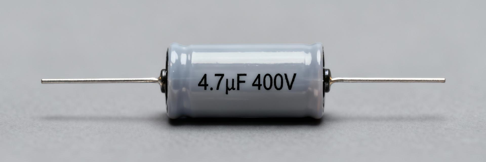
Point: The device is a metallized polyester film capacitor rated nominally 4.7 µF with ~400 V class voltage capability suitable for many power electronics roles. Evidence: Typical parts in this family show low profile radial leads and compact volumetric penalty vs. electrolytics. Explanation: For DC‑link or snubber use, designers choose these for stable capacitance at mid frequencies, low ESR relative to older film types, and good self‑healing under transient stress.
What this part is and typical application areas
Point: This part is a metallized polyester film capacitor intended for pulse and smoothing functions. Evidence: Typical applications include DC‑link smoothing, EMI/RFI suppression, and snubber networks near switching nodes. Explanation: Its nominal capacitance and voltage class favor energy buffering at switching frequencies where electrolytics may degrade; designers should expect capacitance vs. frequency roll‑off and plan parallelization for bulk energy needs.
Quick spec snapshot (table-ready items)
Point: A concise table of datasheet rows clarifies selecting and laying out the part. Evidence: Each table row links to deeper analysis in later sections (electrical behavior, mechanical footprint, reliability). Explanation: Use the table to match system constraints (voltage, ripple, footprint) before detailed thermal calculations.
| Parameter | Typical Entry |
|---|---|
| Capacitance | 4.7 µF ±10% |
| Rated Voltage | 400 V DC (AC rating per vendor) |
| Dielectric | Metallized polyester |
| Dissipation Factor / ESR | Low (specified on datasheet) |
| Ripple Current | Refer to datasheet table / frequency |
| Temperature Range | Typical class −55 °C to +125 °C |
| Case / Lead Spacing | 2‑pin radial, dimensions on mechanical drawing |
| RoHS | Compliant (check lot certificate) |
(2) Complete Electrical Specifications (Datasheet Breakdown) [Data analysis]
Point: The electrical section decodes capacitance behavior, voltage limits and loss mechanisms from the datasheet. Evidence: Datasheet tables list nominal C, tolerance, DF (or ESR), rated voltages, and ripple allowances. Explanation: Read the tables to extract temperature coefficients, frequency dependence and the dissipation factor to estimate heating under AC ripple; those numbers drive derating and parallelization choices.
Capacitance, tolerance, and temperature behavior
Point: Nominal 4.7 µF with ±10% tolerance governs effective decoupling bandwidth. Evidence: Metallized polyester shows reduced capacitance with frequency and modest negative temperature coefficient. Explanation: Expect several percent loss at high frequency and a few percent aging per 1,000 hours; verify required low‑frequency bulk with parallel higher‑capacitance parts if needed.
- Actionable: Measure capacitance at expected operating temperature and switching frequency; use measured value in time‑constant and ripple calculations.
Voltage ratings, ripple current, dissipation factor and ESR
Point: Rated DC/AC voltages and DF/ESR determine allowable ripple and thermal rise. Evidence: Datasheet ripple current (when provided) and DF allow power loss P = I_rms^2 × ESR approximation. Explanation: Use P = I_rms^2 × ESR to get dissipation, then ΔT ≈ P × thermal resistance to estimate temperature rise and ensure operation below maximum temperature.
- Example calculation: For 1.0 A ripple and ESR = 0.5 Ω, P = 0.5 W; ensure thermal path and derating to keep ΔT within datasheet limits.
(3) Physical, Mechanical & Environmental Specs [Data analysis]
Point: Mechanical drawings and packaging determine footprint, lead length and assembly behavior. Evidence: Datasheet mechanical sheet provides dimensions, tolerances and lead spacing. Explanation: Verify PCB pad pattern, allow for lead bending stresses, and choose taped packaging for automated insertion or bulk for manual assembly.
Dimensions, lead format, packaging and footprint considerations
Point: Typical form factor is 2‑pin radial with defined lead spacing and body outline. Evidence: Mechanical tolerances inform solder fillet and standoff requirements. Explanation: Design pads with 20–30% extra solder fillet area, maintain short connection loops for low inductance, and plan mechanical support for heavy axial loads.
- PCB tip: Keep lead length minimal, add a retention pad or glue for vibration environments.
Temperature range, aging, and reliability expectations
Point: Operating limits and aging rates affect long‑term capacitance and breakdown risk. Evidence: Class specifications typically list operating ranges and recommended derating. Explanation: Apply voltage derating (e.g., 80% of rated DC for continuous operation) and reduce maximum ambient to extend life; include thermal cycling and humidity tests in qualification.
- Rule of thumb: Derate voltage and reduce ripple to improve life; schedule accelerated life tests to quantify aging for your system.
(4) How to Choose & Integrate B32564J6475K000 in Your Design [Method \/ selection guide]
Point: Selection requires balancing capacitance, voltage margin, ripple handling and ESR. Evidence: Datasheet and system simulation indicate required values. Explanation: Use a checklist to confirm C, tolerance, voltage derating, ripple, ESR, and temperature before layout and testing.
Electrical selection checklist
Point: A stepwise checklist ensures pass/fail decisions are data‑driven. Evidence: Compare required energy buffering, allowable ΔV, and expected ripple current vs. datasheet entries. Explanation: For paralleling N identical caps to share ripple, divide required I_ripple by N and recompute heating per device; requalify at assembly level.
- Checklist: required C and tolerance → voltage derating → ripple per device → ESR/DF limits → temperature profile → safety/EMI needs.
PCB layout and EMI\/performance tips
Point: Layout strongly affects effective impedance and EMI. Evidence: Short traces and low loop area reduce common‑mode and differential emissions. Explanation: Place film capacitor close to switching node, use wide traces, provide Kelvin current return if measuring ESR, and include test pads for in‑circuit validation.
- Tip: Use parallel small film caps for high‑frequency decoupling and one larger film for energy buffering to smooth ripple across bandwidth.
(5) Mounting, Testing, Reliability and Safety Best Practices [Method \/ best practices]
Point: Proper assembly and test regimes prevent early failures. Evidence: Datasheet mechanical notes and reliability tables recommend solder profiles and handling limits. Explanation: Avoid excessive heat during soldering, support heavy parts mechanically, and follow recommended creepage/clearance for high‑voltage assemblies.
Assembly, soldering and safety precautions
Point: Lead bending and soldering profiles protect dielectric and metallization. Evidence: Standard practice limits hand‑soldering temperature and dwell. Explanation: Preform leads with controlled bends, limit hand‑solder dwell to recommended seconds, and provide strain relief to avoid fatigue under vibration.
- Safety: Ensure adequate clearance and insulation for high‑voltage rails; follow agency spacing guidelines in final product.
Verification tests and failure modes to watch
Point: Bench tests confirm in‑system behavior and detect common failure modes. Evidence: LCR, DC leakage, thermal profiling under designed ripple, and surge tests reveal degradation. Explanation: Watch for loss of capacitance, increased DF, or insulation breakdown; use IR and high‑pot tests as appropriate for safety qualification.
- Recommended tests: LCR sweep at operating frequency, leakage current at rated voltage, thermal rise under ripple, accelerated humidity and thermal cycling.
(6) Sourcing, Alternatives & Cost Considerations [Case \/ action recommendations]
Point: Verify full part code and cross‑reference electrical and mechanical parity when selecting substitutes. Evidence: Matching capacitance, voltage, dielectric type, ESR/DF and footprint minimizes requalification. Explanation: Accept substitutes only after system‑level testing; prioritize lot traceability, RoHS certificates and lead time planning for production.
Where to confirm part details and choosing substitutes
Point: Cross‑reference by electrical and mechanical parameters rather than just part code. Evidence: Equivalent film capacitor types will share dielectric and ESR ranges. Explanation: For substitutes, match C, tolerance, voltage, DF/ESR, dimensions and temperature rating; run at‑system tests to confirm thermal and EMI performance.
- Substitute criteria: C ± tolerance, voltage rating ≥ original derated value, ESR/DF within acceptable range, mechanical fit, and equivalent reliability classification.
Procurement checklist and lifecycle tips
Point: Stocking strategy and lot control reduces production risk. Evidence: Lead time variability and lot differences can affect availability. Explanation: Maintain safety stock for production, document lot certificates, and plan requalification for long‑life products if changing material grade or vendor.
Summary (actionable recap)
Key takeaway: Use datasheet numeric entries (capacitance, voltage, DF, ripple) to drive voltage derating, thermal estimates and parallelization decisions for B32564J6475K000. Confirm mechanical fit, plan PCB layout to minimize loop inductance, and require in‑system verification to finalize a substitute or procurement decision.
Key summary
- Match primary specs: 4.7 µF at rated voltage, tolerance and DF — verify actual capacitance at operating frequency before finalizing designs using the datasheet tables.
- Ripple and heating: compute P = I_rms^2 × ESR to estimate temperature rise and apply voltage derating to extend life; parallelize to share ripple if needed.
- Mechanical & assembly: design PCB pads for minimal lead length, provide mechanical support for vibration, and follow soldering limits to avoid dielectric damage.
- Procurement & qualification: confirm lot traceability and RoHS status, maintain safety stock, and perform accelerated tests when changing sources for long‑life products.
Common questions
What is the voltage rating and capacitance of B32564J6475K000?
The nominal capacitance is 4.7 µF with typical ±10% tolerance; the part number denotes a 400 V class nominal rating for DC applications. Check the datasheet mechanical and voltage tables for AC ratings and any application‑specific derating guidance before committing to production use.
How do I calculate ripple heating for a 4.7 µF, 400 V film capacitor?
Estimate heating with P = I_rms^2 × ESR (or P ≈ I_rms^2 × DF / (2πfC) when ESR not given). Compute ΔT from P using the part’s thermal resistance to ambient; ensure operating temperature stays below the maximum specified in the datasheet after accounting for ambient and internal heating.
When should I parallel multiple film capacitors for higher ripple current?
Parallel when single‑part ripple rating or ESR constraints are exceeded. Divide the required ripple current by the number of caps to determine per‑device stress, then verify each device’s temperature rise and lifetime via thermal testing. Requalify the parallel network for EMI and resonance effects in the system.
- Technical Features of PMIC DC-DC Switching Regulator TPS54202DDCR
- STM32F030K6T6: A High-Performance Core Component for Embedded Systems
- Tamura L34S1T2D15 Datasheet Breakdown: Key Specs & Limits
- PAL6055.700HLT Datasheet: Complete Technical Report
- FDP027N08B MOSFET Datasheet Deep-Dive: Key Specs & Test Data
- LT1074IT7: Complete Specs & Key Parameters Breakdown
- How to Verify G88MP061028 Datasheet and Specs - Checklist
- NFAQ0860L36T Datasheet: Measured IPM Performance Report
- 90T03P MOSFET: Complete Specs, Pinout & Ratings Digest
- 3386F-1-101LF Datasheet & Specs — Pinout, Ratings, Sources
-
 MM74HC4050NSanyo Semiconductor/onsemiIC BUFFER NON-INVERT 6V 16DIP
 -
 MM74HC4049NSanyo Semiconductor/onsemiIC BUFFER NON-INVERT 6V 16DIP
 -
 MM74HC4040NSanyo Semiconductor/onsemiIC BINARY COUNTER 12-BIT 16DIP
 -
 MM74HC4020NSanyo Semiconductor/onsemiIC BINARY COUNTER 14-BIT 16DIP
 -
 MM74HC393NSanyo Semiconductor/onsemiIC BINARY COUNTR DL 4BIT 14MDIP
 -
 MM74HC374NSanyo Semiconductor/onsemiIC FF D-TYPE SNGL 8BIT 20DIP
 -
 MM74HC373NSanyo Semiconductor/onsemiIC D-TYPE TRANSP SGL 8:8 20DIP
 -
 LT1213CS8Linear Technology (Analog Devices, Inc.)IC OPAMP GP 2 CIRCUIT 8SO
 -
 MM74HC259NSanyo Semiconductor/onsemiIC LATCH ADDRESS 8BIT 16-DIP
 -
 MM74HC251NSanyo Semiconductor/onsemiIC MULTIPLEXER 1 X 8:1 16DIP

