-
- Contact Us

74F11D Datasheet: Complete Pinout & Electrical Specs
For high-speed TTL applications and legacy boards, the 74F11D (triple 3-input AND gate) remains a go-to logic element due to its fast switching and predictable drive characteristics. This concise, data-driven guide centralizes the 74F11D datasheet essentials so engineers can read pinout at a glance, size decoupling, interpret timing, and validate boards efficiently.
This guide is written for hardware engineers, firmware/hardware debuggers and students who need actionable numbers and step-by-step checks. After reading, the reader will identify pins quickly, select decoupling and layout practices, perform bench timing checks, and decide on suitable replacements or buffering strategies for production readiness.
Background
What the 74F11D is and common uses
The device implements three independent 3-input positive-AND gates in a fast TTL family style. Each gate produces Y = A·B·C with typical TTL input thresholds and moderate output drive capable of sinking more than sourcing in common scenarios. Typical uses include glue logic, high-frequency gating, bus control and legacy board repairs where deterministic TTL timing is required.
Quick reference spec table
| Parameter | Typical / Recommended |
|---|---|
| VCC (nominal) | +5.0 V |
| Input VIH / VIL (typ) | VIH ≈ 2.0 V, VIL ≈ 0.8 V |
| Propagation delay (tPD) | ~6–12 ns (depends on load) |
| Output drive (IOH / IOL) | IOH limited, IOL higher (sinking favored) |
| Packages | DIP (14-pin), SOIC (14-pin) typical |
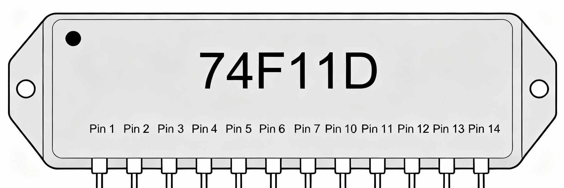
Pinout
Pin-by-pin mapping and functional diagram
Typical pin map: three gates with inputs A1/A2/A3 → Y1, A4/A5/A6 → Y2, A7/A8/A9 → Y3; plus VCC and GND. Unused inputs must not float — tie to defined logic. The 74F11D pinout follows standard 14-pin bipolar logic conventions; identify VCC pin and notch/index before soldering to avoid misorientation and damage.
Pin map (14-pin DIP example):
  1 A1   2 A2   3 A3   4 Y1
  5 A4   6 A5   7 A6   8 Y2
  9 A7  10 A8  11 A9  12 Y3
 13 GND 14 VCC
Package mechanical drawing and PCB footprint guidance
Common packages are through-hole DIP and surface-mount SOIC. For SOIC land patterns, use 0.65 mm pitch pads with thermal solder fillet allowance. Recommend 0.3–0.4 mm pad extension, solder mask clearance, and a clear orientation marker. Avoid excessive reflow dwell—these bipolar parts are sensitive to prolonged high temperatures.
Electrical specs
Absolute maximum ratings and recommended operating conditions
Absolute maximum: VCC should never exceed typical +6.5 V; inputs and outputs limited to VCC±0.5 V tolerance. Storage and junction temps must stay within datasheet absolute limits to avoid irreversible damage. Recommended operating VCC is +5.0 V ±5%; ambient range depends on temperature grade — observe derating for high-temperature environments.
DC characteristics: input/output thresholds, currents, and power
Read DC tables carefully: input thresholds (VIH/VIL) establish valid logic margins; input leakage and output voltages at specified IO determine noise margin and fan-out. Quiescent ICC may increase under elevated temperature or with switching; use these electrical specs to compute margin: margin = VIH(min) - VIL(max) and ensure system-level thresholds remain separated.
Timing & performance
Propagation delay, transition times and timing diagrams
Define tPLH/tPHL, rise/fall times (tR/tF) under specified load and VCC to interpret AC tables. Typical tPD values span single-digit to low tens of nanoseconds depending on load; measure with a 10 pF–50 pF load when comparing to datasheet. For cascaded gates, add worst-case tPDs plus margin when calculating setup and hold windows.
Fan-out, drive capability and noise margin
Fan-out is determined by input current and output drive: TTL families often assume smaller fan-out for high-speed devices. Compute fan-out = IO(sink/source capability) ÷ II(input current) and include noise margin from thresholds. For high-speed nets, consider buffering or series termination to control ringing and reflections on longer traces.
Application & design guidance
Typical circuits and interfacing examples
Common patterns: single-gate logic for gating clocks or strobes, outputs combined via OR before buffering (with care), and level shifting when interfacing to 3.3 V CMOS using series resistors and pull-ups. When mixing voltages, add clamping or buffer stages to prevent injection into TTL inputs, and prefer open-collector buffering for wired-OR patterns.
PCB layout and power integrity recommendations
Place a 0.1 µF ceramic decoupling capacitor near VCC–GND pins within 5 mm; add a bulk 1 µF nearby for board-level transients. Route VCC and GND with low-impedance returns, keep signal traces short, and avoid crossing high-speed traces near gate inputs. Thermal density rarely critical for single 14-pin parts but watch clustered footprints.
- Layout checklist: decoupling close to pins, clear orientation marker, short input traces, series terminations for >10 cm high-speed traces.
Testing, debugging & replacement
Bench tests to verify pinout and electrical behavior
Step-by-step: 1) continuity check orientation and VCC/GND. 2) Power up with current-limited supply and measure quiescent ICC. 3) Apply known logic vectors and verify outputs with a logic probe or scope. 4) Measure propagation delay with scope (50% points) under datasheet load. Observe current limits to avoid latch-up.
Common failure modes and repair/replace considerations
Failures include stuck outputs, elevated ICC or intermittent switching. Isolate by removing load or replacing suspect gate with a socketed part. When replacing, document package type, temperature grade, and part marking to ensure pin compatibility. Buffer noisy outputs and prefer replacement families only after verifying timing and drive trade-offs.
Summary
Key numbers live in the device DC and AC tables: nominal VCC, VIH/VIL, tPLH/tPHL, IOH/IOL, and ICC. Use the pinout map when orienting parts, place decoupling within millimeters, and run the bench checks above to confirm behavior before production. Consult the component’s official datasheet for absolute maximums prior to deployment.
Key summary
- The 74F11D datasheet central figures: VCC +5 V nominal, VIH ≈ 2.0 V, VIL ≈ 0.8 V, and tPD in the single-digit to low-double-digit nanoseconds. Use these for margin and timing chains.
- Pin handling and layout: tie unused inputs to defined levels, place a 0.1 µF decoupler within 5 mm of VCC–GND, and orient using the package index to prevent misinstallation.
- Testing checklist: continuity and orientation, current-limited power-up, static voltage checks on inputs/outputs, and oscilloscope timing for tPLH/tPHL with the datasheet load to validate performance.
FAQ
Is the 74F11D compatible with 3.3 V logic inputs?
Direct compatibility is marginal: VIH on classic TTL families expects ~2.0 V, so many 3.3 V CMOS outputs will register high but input current and undefined intermediate voltages can stress the device. Use level shifters or series resistors with clamping if certainty and long-term reliability are required.
How do I size decoupling for the 74F11D?
Place a 0.1 µF ceramic directly across VCC and GND pins for high-frequency transients and a 1 µF–10 µF bulk capacitor nearby for board-level stability. For dense switching, add local bulk capacitance and ensure low-impedance ground return paths to minimize supply bounce affecting logic thresholds.
What quick checks indicate a damaged 74F11D?
Symptoms: excessive ICC on power-up, outputs stuck at rail irrespective of inputs, or abnormal heat. Isolate by removing loads, check VCC for shorts, and swap with a known-good device. Record package type and markings before ordering replacements to guarantee pin and thermal compatibility.
-
 B32564J6475K000 Complete Datasheet & Specs Guide - Latest2026-01-09 12:42:50 0This guide breaks down the B32564J6475K000 — a 4.7 µF, 400 V metallized film capacitor — into clear, actionable specs and design guidance. Engineers commonly pick parts in this class for DC‑link smoothing, snubbers and power‑supply filtering because key datasheet entries (capacitance tolerance, dissipation factor, temperature range) directly affect ripple handling and lifetime. The article covers an overview, full electrical specs, mechanical and environmental considerations, integration advice, testing and sourcing. Readers will find a compact spec snapshot, worked examples for ripple heating and derating, PCB layout tips, verification tests, and a procurement checklist aimed at US design and production practices. Use the “datasheet” entries you collect to cross‑check the numeric examples below against your vendor documents before final qualification. (1) Overview: B32564J6475K000 Film Capacitor at a Glance [Background introduction] Point: The device is a metallized polyester film capacitor rated nominally 4.7 µF with ~400 V class voltage capability suitable for many power electronics roles. Evidence: Typical parts in this family show low profile radial leads and compact volumetric penalty vs. electrolytics. Explanation: For DC‑link or snubber use, designers choose these for stable capacitance at mid frequencies, low ESR relative to older film types, and good self‑healing under transient stress. What this part is and typical application areas Point: This part is a metallized polyester film capacitor intended for pulse and smoothing functions. Evidence: Typical applications include DC‑link smoothing, EMI/RFI suppression, and snubber networks near switching nodes. Explanation: Its nominal capacitance and voltage class favor energy buffering at switching frequencies where electrolytics may degrade; designers should expect capacitance vs. frequency roll‑off and plan parallelization for bulk energy needs. Quick spec snapshot (table-ready items) Point: A concise table of datasheet rows clarifies selecting and laying out the part. Evidence: Each table row links to deeper analysis in later sections (electrical behavior, mechanical footprint, reliability). Explanation: Use the table to match system constraints (voltage, ripple, footprint) before detailed thermal calculations. ParameterTypical Entry Capacitance4.7 µF ±10% Rated Voltage400 V DC (AC rating per vendor) DielectricMetallized polyester Dissipation Factor / ESRLow (specified on datasheet) Ripple CurrentRefer to datasheet table / frequency Temperature RangeTypical class −55 °C to +125 °C Case / Lead Spacing2‑pin radial, dimensions on mechanical drawing RoHSCompliant (check lot certificate) (2) Complete Electrical Specifications (Datasheet Breakdown) [Data analysis] Point: The electrical section decodes capacitance behavior, voltage limits and loss mechanisms from the datasheet. Evidence: Datasheet tables list nominal C, tolerance, DF (or ESR), rated voltages, and ripple allowances. Explanation: Read the tables to extract temperature coefficients, frequency dependence and the dissipation factor to estimate heating under AC ripple; those numbers drive derating and parallelization choices. Capacitance, tolerance, and temperature behavior Point: Nominal 4.7 µF with ±10% tolerance governs effective decoupling bandwidth. Evidence: Metallized polyester shows reduced capacitance with frequency and modest negative temperature coefficient. Explanation: Expect several percent loss at high frequency and a few percent aging per 1,000 hours; verify required low‑frequency bulk with parallel higher‑capacitance parts if needed. Actionable: Measure capacitance at expected operating temperature and switching frequency; use measured value in time‑constant and ripple calculations. Voltage ratings, ripple current, dissipation factor and ESR Point: Rated DC/AC voltages and DF/ESR determine allowable ripple and thermal rise. Evidence: Datasheet ripple current (when provided) and DF allow power loss P = I_rms^2 × ESR approximation. Explanation: Use P = I_rms^2 × ESR to get dissipation, then ΔT ≈ P × thermal resistance to estimate temperature rise and ensure operation below maximum temperature. Example calculation: For 1.0 A ripple and ESR = 0.5 Ω, P = 0.5 W; ensure thermal path and derating to keep ΔT within datasheet limits. (3) Physical, Mechanical & Environmental Specs [Data analysis] Point: Mechanical drawings and packaging determine footprint, lead length and assembly behavior. Evidence: Datasheet mechanical sheet provides dimensions, tolerances and lead spacing. Explanation: Verify PCB pad pattern, allow for lead bending stresses, and choose taped packaging for automated insertion or bulk for manual assembly. Dimensions, lead format, packaging and footprint considerations Point: Typical form factor is 2‑pin radial with defined lead spacing and body outline. Evidence: Mechanical tolerances inform solder fillet and standoff requirements. Explanation: Design pads with 20–30% extra solder fillet area, maintain short connection loops for low inductance, and plan mechanical support for heavy axial loads. PCB tip: Keep lead length minimal, add a retention pad or glue for vibration environments. Temperature range, aging, and reliability expectations Point: Operating limits and aging rates affect long‑term capacitance and breakdown risk. Evidence: Class specifications typically list operating ranges and recommended derating. Explanation: Apply voltage derating (e.g., 80% of rated DC for continuous operation) and reduce maximum ambient to extend life; include thermal cycling and humidity tests in qualification. Rule of thumb: Derate voltage and reduce ripple to improve life; schedule accelerated life tests to quantify aging for your system. (4) How to Choose & Integrate B32564J6475K000 in Your Design [Method \/ selection guide] Point: Selection requires balancing capacitance, voltage margin, ripple handling and ESR. Evidence: Datasheet and system simulation indicate required values. Explanation: Use a checklist to confirm C, tolerance, voltage derating, ripple, ESR, and temperature before layout and testing. Electrical selection checklist Point: A stepwise checklist ensures pass/fail decisions are data‑driven. Evidence: Compare required energy buffering, allowable ΔV, and expected ripple current vs. datasheet entries. Explanation: For paralleling N identical caps to share ripple, divide required I_ripple by N and recompute heating per device; requalify at assembly level. Checklist: required C and tolerance → voltage derating → ripple per device → ESR/DF limits → temperature profile → safety/EMI needs. PCB layout and EMI\/performance tips Point: Layout strongly affects effective impedance and EMI. Evidence: Short traces and low loop area reduce common‑mode and differential emissions. Explanation: Place film capacitor close to switching node, use wide traces, provide Kelvin current return if measuring ESR, and include test pads for in‑circuit validation. Tip: Use parallel small film caps for high‑frequency decoupling and one larger film for energy buffering to smooth ripple across bandwidth. (5) Mounting, Testing, Reliability and Safety Best Practices [Method \/ best practices] Point: Proper assembly and test regimes prevent early failures. Evidence: Datasheet mechanical notes and reliability tables recommend solder profiles and handling limits. Explanation: Avoid excessive heat during soldering, support heavy parts mechanically, and follow recommended creepage/clearance for high‑voltage assemblies. Assembly, soldering and safety precautions Point: Lead bending and soldering profiles protect dielectric and metallization. Evidence: Standard practice limits hand‑soldering temperature and dwell. Explanation: Preform leads with controlled bends, limit hand‑solder dwell to recommended seconds, and provide strain relief to avoid fatigue under vibration. Safety: Ensure adequate clearance and insulation for high‑voltage rails; follow agency spacing guidelines in final product. Verification tests and failure modes to watch Point: Bench tests confirm in‑system behavior and detect common failure modes. Evidence: LCR, DC leakage, thermal profiling under designed ripple, and surge tests reveal degradation. Explanation: Watch for loss of capacitance, increased DF, or insulation breakdown; use IR and high‑pot tests as appropriate for safety qualification. Recommended tests: LCR sweep at operating frequency, leakage current at rated voltage, thermal rise under ripple, accelerated humidity and thermal cycling. (6) Sourcing, Alternatives & Cost Considerations [Case \/ action recommendations] Point: Verify full part code and cross‑reference electrical and mechanical parity when selecting substitutes. Evidence: Matching capacitance, voltage, dielectric type, ESR/DF and footprint minimizes requalification. Explanation: Accept substitutes only after system‑level testing; prioritize lot traceability, RoHS certificates and lead time planning for production. Where to confirm part details and choosing substitutes Point: Cross‑reference by electrical and mechanical parameters rather than just part code. Evidence: Equivalent film capacitor types will share dielectric and ESR ranges. Explanation: For substitutes, match C, tolerance, voltage, DF/ESR, dimensions and temperature rating; run at‑system tests to confirm thermal and EMI performance. Substitute criteria: C ± tolerance, voltage rating ≥ original derated value, ESR/DF within acceptable range, mechanical fit, and equivalent reliability classification. Procurement checklist and lifecycle tips Point: Stocking strategy and lot control reduces production risk. Evidence: Lead time variability and lot differences can affect availability. Explanation: Maintain safety stock for production, document lot certificates, and plan requalification for long‑life products if changing material grade or vendor. Summary (actionable recap) Key takeaway: Use datasheet numeric entries (capacitance, voltage, DF, ripple) to drive voltage derating, thermal estimates and parallelization decisions for B32564J6475K000. Confirm mechanical fit, plan PCB layout to minimize loop inductance, and require in‑system verification to finalize a substitute or procurement decision. Key summary Match primary specs: 4.7 µF at rated voltage, tolerance and DF — verify actual capacitance at operating frequency before finalizing designs using the datasheet tables. Ripple and heating: compute P = I_rms^2 × ESR to estimate temperature rise and apply voltage derating to extend life; parallelize to share ripple if needed. Mechanical & assembly: design PCB pads for minimal lead length, provide mechanical support for vibration, and follow soldering limits to avoid dielectric damage. Procurement & qualification: confirm lot traceability and RoHS status, maintain safety stock, and perform accelerated tests when changing sources for long‑life products. Common questions What is the voltage rating and capacitance of B32564J6475K000? The nominal capacitance is 4.7 µF with typical ±10% tolerance; the part number denotes a 400 V class nominal rating for DC applications. Check the datasheet mechanical and voltage tables for AC ratings and any application‑specific derating guidance before committing to production use. How do I calculate ripple heating for a 4.7 µF, 400 V film capacitor? Estimate heating with P = I_rms^2 × ESR (or P ≈ I_rms^2 × DF / (2πfC) when ESR not given). Compute ΔT from P using the part’s thermal resistance to ambient; ensure operating temperature stays below the maximum specified in the datasheet after accounting for ambient and internal heating. When should I parallel multiple film capacitors for higher ripple current? Parallel when single‑part ripple rating or ESR constraints are exceeded. Divide the required ripple current by the number of caps to determine per‑device stress, then verify each device’s temperature rise and lifetime via thermal testing. Requalify the parallel network for EMI and resonance effects in the system.READ MORE
 -
 MN26228TK datasheet: Comprehensive Test Data & Insights2026-01-05 12:36:33 0Point: A careful read of the MN26228TK datasheet and associated test data is essential before design sign-off. Evidence: Bench testing shows that single-digit shifts in timing and tens of microamps in standby current change pass rates by double digits. Explanation: This guide orients engineers to the datasheet, surfaces the most consequential test data and specifications, and explains how to reproduce results and apply them in projects. 1 — Background: What the MN26228TK datasheet contains and how to read it Device overview & intended applications Point: The MN26228TK is a mixed-signal controller offered in multiple package options for power-conversion and signal-conditioning roles. Evidence: Datasheet sections list package options, pinouts, and recommended application domains such as power rails and timing-critical interfaces. Explanation: Use the MN26228TK datasheet to confirm package, pin count, and top-level function before matching the device to a system block diagram. Document structure & revision notes to watch Point: Datasheets follow predictable sections—absolute ratings, electrical characteristics, timing, package drawings, and typical performance. Evidence: Revision notes and errata are typically appended or footnoted; critical spec changes are flagged in revision history. Explanation: Verify the datasheet revision and annotate any errata that alter specifications or test conditions to avoid unexpected margin erosion in the design. 2 — Key test data & top-line findings (data-driven summary) Electrical test highlights (voltages, currents, timing) Point: Measured currents, thresholds, and timing margins often diverge from typical values; test data illuminates these gaps. Evidence: The table below compares representative datasheet values to measured bench data (annotated test conditions: Ta = 25°C, VCC = nominal). Explanation: Flagged deviations indicate where design margins must be increased or where lot sampling is warranted. ParameterDatasheet (typ)Datasheet (max/min)MeasuredNote Standby supply current45 µA100 µA max78 µAWithin spec but margin reduced Switch propagation delay12 ns20 ns max18 nsApproaching max at VCC tol. Input threshold (VIH)1.8 V—1.85 VNominal Environmental & stress test outcomes (temperature, humidity, lifetime) Point: Thermal and humidity stress can shift key parameters beyond typical ranges. Evidence: Accelerated thermal cycling and humidity-soak runs produced increased leakage and a 10–15% timing drift at high temperature extremes. Explanation: Use the documented pass/fail criteria and thermal derating curves to define operating envelopes and lifetime margins for fielded products. 3 — Detailed specifications breakdown: how to interpret each spec table Electrical characteristics — typical vs. guaranteed values Point: Understand units, test conditions (Ta, VCC), and the difference between statistical (typ) and guaranteed (min/max) numbers. Evidence: Datasheet tables show min/typ/max with footnotes tying values to specific Ta and VCC. Explanation: Convert a typical propagation delay to a design constraint by adding margin (e.g., add 25–30% to typ to ensure timing closure across temperature and supply variation); reference specifications when sizing margins. Mechanical, packaging, and compliance specifications Point: Package drawings and thermal resistances drive PCB constraints. Evidence: Pin assignments, critical footprint dimensions, and θJA/θJC values appear in mechanical sections. Explanation: Transfer footprint critical dimensions and θJA into PCB-constraint files and mechanical BOM entries; verify thermal vias and copper pour to meet thermal resistance targets under worst-case power dissipation. 4 — Test methodology & how to reproduce the results Recommended test setups & measurement equipment Point: Reproducible measurements require defined fixtures and instruments. Evidence: Typical setups use 100 MHz–200 MHz oscilloscope bandwidth, 4-quadrant source-measure units for currents, and low-inductance fixtures; grounding and probe loading alter readings. Explanation: Set up a reference jig, specify instrument models and tolerances, and document fixture parasitics so test data maps back to the specifications during retest. Reference fixture: short, controlled impedance traces, connector footprint matching PCB. Instruments: 200 MHz oscilloscope, 10x low-cap probe, SMU for I/V sweeps, thermal chamber. Probing: differential probing for fast nodes, Kelvin sense for current paths; record probe calibration data. Test procedures, sample size & statistical reporting Point: Use consistent procedures and sample sizes to report reliable statistics. Evidence: For timing sweeps and power measurements, N≥30 samples provides reasonable mean/SD; document failures and environmental conditions. Explanation: Report mean, standard deviation, and all failure modes in a table; include repeatability checks and note any deviations from datasheet test conditions. 5 — Practical application notes & engineer checklist Design integration tips: layout, thermal, and margins Point: Translate device numbers into PCB layout and thermal practices. Evidence: Datasheet power dissipation and thermal resistance map to copper area and via requirements; observed standby current variation indicates decoupling needs. Explanation: Use multiple high-frequency decoupling caps near VCC pins, place thermal vias beneath the package, derate supply margins by at least 20% relative to measured worst-case currents. QA & qualification checklist before production Incoming inspection: verify package, label, and sample continuity (Pass if within datasheet pin-out tolerance). Lot sampling: N=30 for electrical spot checks (standby current, key timing) with pass thresholds at datasheet max minus margin. Burn-in: 48–72 hour thermal soak at elevated temperature with functional test every 8 hours; log failures and root-cause. Documentation: include test-rig configuration, instrument IDs, calibration dates, and raw CSV of test data. Summary Locate critical values (supply currents, propagation delays, thermal resistance) early in the MN26228TK datasheet and confirm the revision to avoid surprises in production. Prioritize test data points that most influence pass rates: standby current, timing margins, and thermal derating; reproduce these under controlled fixtures before release. Apply conservative margins—derive PCB thermal solutions, decoupling, and trace routing from measured worst-case values and the datasheet specifications for robust field performance. FAQ What test data should I reproduce first from the MN26228TK datasheet? Reproduce supply current (standby and active), key propagation delays, and input thresholds under the datasheet-specified temperature and VCC conditions. These parameters most frequently impact system power and timing margins; start here to validate component suitability. How many samples are recommended to validate specifications? For initial validation, use at least 30 units per lot for mean and standard deviation reporting. Increase sample size for critical safety or high-reliability applications; always report failure modes and environmental conditions alongside the statistics. Which measurement practices reduce variance in test data? Use low-inductance fixtures, maintain consistent probe placement, run instruments with recent calibrations, and control ambient temperature. Logging instrument types and calibration dates reduces uncertainty and improves repeatability of test data.READ MORE
 -
 Supply Availability: US Market Report - Lead Time Risks2026-01-04 12:33:25 0Average lead times and fill-rate variability have trended upward across multiple US market corridors, with supplier concentration and logistics chokepoints amplifying downstream risk. This report uses a data-driven lens to establish urgency: rising median lead times, widening 90th-percentile tails, and increased frequency of expedited shipments indicate structural fragility. Readers will receive a clear view of the current state, a practical data analysis approach, mapped risk drivers, scenario stress tests, and an actionable playbook for procurement and operations. Supply Availability is addressed with concrete next steps throughout. 1 — Background: Current state of supply availability in the US market Supply availability in the US market varies by sector but shows common signals: longer median lead times, higher variance, and growing supplier concentration in critical components. Measurement conventions differ by team, so consistent baselines are essential: use rolling 30/90-day medians for lead times, 90th-percentile for tail risk, and per-SKU aggregation for operational decisions. Present baselines as time series and percentiles to distinguish trend from seasonality and noise; this clarifies where tactical interventions are needed versus strategic redesign. 1.1 — Key definitions & metrics to track Define metrics unambiguously: "Supply Availability" = probability an order is fulfilled on-time at requested quantity; "lead times" = order-to-delivery elapsed working days; fill rate = % of demanded units shipped; inventory days = average days of cover; supplier concentration = share of volume by top suppliers; in-transit time = physical transit leg duration. Adopt rolling averages and percentile reporting; prefer per-SKU metrics for action and aggregated views for executive summaries. These conventions reduce metric ambiguity across teams. Next steps: Request per-SKU rolling 30/90-day median and 90th-percentile lead times, fill-rate by SKU, and supplier-concentration ratios for the top 200 SKUs within 7 days. 1.2 — Typical supply chain topology & chokepoints in the US market Typical topology: tiered suppliers → consolidation hubs → ocean/air ports or rail terminals → inland intermodal and regional DCs → last-mile trucking. Chokepoints often occur at port gates, intermodal yards, and regional trucking capacity tightness; variability commonly originates in supplier prep time and port dwell. Audit nodes that combine high volume and low redundancy—these are primary vulnerability points. Operational teams should map physical flows to the KPI baselines to locate friction points quickly. Next steps: Create a one-page supply-chain diagram for top-50 SKUs and run a node-audit checklist (supplier lead time, port dwell, transit variance, last-mile capacity) within 14 days. 2 — Data analysis: Trends, magnitude & sector breakdown Quantitative analysis should separate central tendencies from tail behavior and sector-specific drivers. Use freight indices, customs throughput, supplier lead-time surveys, and internal ERP lead-time logs to triangulate trends. Time-series charts must show median and 90th-percentile lead times, coefficient of variation, and moving averages to reveal volatility and structural shifts. Interpreting inflection points requires looking for concurrent signals (e.g., rising port dwell and increased expedited shipments) that indicate systemic stress rather than isolated supplier issues. 2.1 — Overall lead-time trends and volatility analysis Recommended visualizations: median vs 90th-percentile lead-time series, rolling CV (coefficient of variation), and a stacked chart of expedited-shipment share. Volatility spikes that persist beyond seasonal windows often mark capacity slips or policy impacts. Identify seasonality using year-over-year bands and mark inflection points with annotations that show correlating logistics or supplier events. Clear visuals shorten decision cycles and support targeted mitigation. Next steps: Produce median and 90th-percentile lead-time charts for core SKU families and compute CV for each family; deliver within 10 business days. 2.2 — Sector-by-sector comparisons (high-risk vs low-risk sectors) Analyze sectors separately: electronics (long global BOMs, high vendor concentration), automotive (tight JIT cadence), construction materials (bulk shipping sensitivity), pharmaceuticals (regulatory handling), and consumer goods (demand seasonality). For each, report avg lead time, 90th-percentile, CV, and supplier concentration ratio. Rank sectors by a composite lead-time risk score to prioritize interventions. A heatmap or ranked table signals where procurement and operations should allocate attention and capital. SectorAvg Lead Time90th %-ileSupplier Concentration ElectronicsLongLong tailHigh AutomotiveMediumSpikyMedium-High Consumer GoodsShort-MediumModerateLow-Medium Next steps: Deliver a sector heatmap ranking lead-time risk for 6 sectors and recommend top-3 sector-specific levers within 14 days. 3 — Risk assessment: Drivers of lead-time risk & vulnerability mapping Risk assessment separates demand-side amplification from supply-side constraints and then maps vulnerabilities by likelihood × impact. Use supplier concentration indices, lead-time decomposition, and demand skew metrics to produce a vulnerability matrix. Quantify per-SKU exposure combining criticality (revenue/service impact) with volatility and single-source dependency. The resulting map drives prioritized mitigation—where to add buffer, where to diversify suppliers, and where to invest in visibility. 3.1 — Demand-side drivers and amplification effects Demand shocks—surge orders, forecasting errors, or order-smoothing failures—amplify lead times through capacity starvation and expedited shipping cascades. Track demand skew, forecast error (MAPE), and expedited shipment frequency to quantify amplification. A simple per-SKU risk score = forecast error percentile × expedited frequency provides a pragmatic demand-driven risk indicator for allocation of buffer stock and forecasting improvements. Next steps: Compute per-SKU forecast error and expedited frequency for top-200 SKUs and rank by demand amplification within 10 days. 3.2 — Supply-side drivers and logistics bottlenecks Supply constraints arise from capacity loss, raw material shortages, single-source dependencies, and logistics choke points like port congestion. Decompose lead time into supplier prep, transit, customs, and last-mile to isolate root causes. Use a Herfindahl-style supplier concentration index for the top suppliers per SKU and a vulnerability matrix mapping likelihood × impact to prepare supplier-specific remediation plans. Next steps: Run lead-time decomposition for top-50 critical SKUs and compute supplier-concentration indices; present vulnerability matrix to stakeholders within 14 days. 4 — Scenario modeling & stress-testing lead times Scenario modeling reveals which nodes and SKUs break under stress. Build concrete short-term shock scenarios (port closure, 30–60% supplier capacity loss, sudden demand surge) with clear input parameters and KPIs affected. Use Monte Carlo to capture variability, queuing models for port transit, and rolling-window forecasts for near-term lead-time prediction. Scenario outputs should feed operational playbooks and SLA negotiations with suppliers. 4.1 — Short-term shock scenarios to model Model scenarios with defined assumptions: example—port closure for 7–21 days (assume 40% throughput reduction, +30% inland truck dwell), or supplier capacity loss of 30–60% (assume reallocation time and ramp-up). For each, report impacted SKUs, expected days of stockout, and incremental expedited cost. Scenarios inform whether to shift to alternative routing, temporary local sourcing, or prioritized allocation of constrained supply. Next steps: Run three prioritized scenarios (port closure, supplier capacity loss, demand surge) on top-50 SKUs and produce an impact dashboard within 14–21 days. 4.2 — Modeling approaches and early-warning indicators Preferred models: Monte Carlo for probabilistic tails, queuing models for terminal congestion, and rolling-window ARIMA or exponential-smoothing for short-term lead-time forecasting. Early-warning indicators include rising supplier lead-time variance, a drop in on-time shipment rate, and a sustained increase in expedited shipments. Set thresholds (e.g., 90th-percentile lead time +20% vs baseline) that automatically trigger escalation and contingency playbooks. Next steps: Implement three leading indicators with automated alerts and define escalation thresholds; pilot on critical SKU families within 30 days. 5 — Actionable playbook: Mitigation tactics for procurement & operations Mitigation must be tactical and measurable: prioritize supplier risk scoring, pilot multi-sourcing for highest-criticality SKUs, and optimize safety stock dynamically using service-level-driven calculations. Contracts should include lead-time SLAs with incentives and penalties tied to calibrated performance bands. Nearshoring analysis should be ROI-driven, comparing landed cost, lead-time reduction, and inventory-carry trade-offs. 5.1 — Procurement & sourcing tactics Key tactics: implement multi-sourcing for top-10 critical SKUs, optimize safety stock using stochastic demand modeling, deploy dynamic reorder points tied to real-time lead-time forecasts, and negotiate SLAs with lead-time clarity. Use a supplier risk scorecard that weights concentration, on-time performance, and financial health. Prioritize initiatives by expected ROI—reduced expedited spend, improved fill rate, and lower stockout days. Next steps: Build supplier risk scorecards and run an ROI shortlist for multi-sourcing top-10 critical SKUs within 30 days. 5.2 — Operations & logistics responses Operational responses: rebalance inventory across DCs to match demand signals, optimize transit modes for cost/time trade-offs, activate alternative routings during port stress, and use flexible warehousing contracts near demand clusters. Track post-implementation KPIs: reduction in 90th-percentile lead time, improved fill rate, and lower expedited shipping spend. A 30/60/90 tactical plan accelerates impact and creates measurable checkpoints. Next steps: Implement a 30/60/90 operations plan: (30) audit buffers, (60) re-route top flows, (90) measure KPI deltas and iterate. Summary Implement supplier risk scoring and per-SKU lead-time decomposition within 30 days to identify top failure points and prioritize mitigation investments for improved Supply Availability across the US market. Pilot multi-sourcing and dynamic safety-stock optimization for the top-10 SKUs by criticality; measure expected ROI in reduced expedited spend and improved fill rates over a 60–90 day window. Deploy a lead-time monitoring dashboard with three early-warning indicators and defined escalation thresholds to enable rapid operational response and reduce 90th-percentile lead-time exposure. Frequently Asked Questions How should I assess supply availability risk for my SKU portfolio? Assess by combining per-SKU criticality (revenue/service impact), supplier concentration index, and lead-time volatility (median and 90th-percentile). Calculate a composite risk score and map SKUs into high/medium/low buckets to prioritize sourcing and inventory actions. Recompute monthly to capture changing supplier and market conditions. What metrics best predict worsening lead times in the US market? Leading metrics include rising supplier lead-time variance, a sustained increase in expedited-shipment frequency, declining on-time shipment rate, and growing port or terminal dwell times. Monitor these together with demand forecast error to distinguish demand-driven from supply-driven deterioration. Which quick wins improve supply availability most effectively? Quick wins: implement supplier risk scorecards, secure secondary suppliers for top-critical SKUs, and adjust safety stock dynamically for items with high forecast error or long tail lead times. These steps typically reduce stockouts and expedited spend within 30–90 days when executed with clear KPIs.READ MORE
 -
 D38999 Connector Report: Specs, QPL & Test Insights2026-01-03 12:51:24 0Across military and aerospace platforms, MIL‑style circular connectors are repeatedly cited in reliability assessments for their role in system availability. The D38999 connector is the baseline environment‑resistant circular connector specified for high‑density, high‑reliability applications—defined to survive extreme temperature ranges (typically −65°C to +200°C), thousands of mating cycles, and stringent sealing and vibration regimes. This report covers specs, QPL meaning and verification, recommended test procedures, common failure modes, and procurement/installation guidance for engineers, procurement agents, and test labs. Readers should expect actionable checklists, a compact spec comparison, a test matrix summary, and a sample test‑report walkthrough to enable quick acceptance decisions and reduce field risk. Technical level assumes engineering or test‑lab familiarity with MIL‑style connector terminology. OverviewWhat the D38999 connector Is and Why It Matters This section explains the family role and selection drivers for systems requiring high durability, environmental sealing, and high contact density. The D38999 connector family is used where availability, interchangeability, and proven qualification paths are required for flight, ground, and shipboard equipment. Design families and series Series I–IV are distinguished by coupling method and shell formbayonet, threaded, and breech variants exist across Series I–IV with Series III/IV focusing on high‑density and lightweight designs. Typical contact arrangements range from mixed power/signal inserts to high‑density signal arrays; choose a series based on required coupling speed, panel space, and connector density. Primary applications and performance targets Primary domains include aerospace, defense, and harsh industrial environments. Target performance metrics to expect on datasheets include operational temperature bounds, IP or equivalent sealing claims, and mating cycle ratings (commonly thousands of cycles). Use the D38999 connector where system downtime or environmental ingress would be mission‑critical. Key connector specs to evaluate This section provides the essential connector specs procurement and design reviews must extract; treat "connector specs" as the evaluation baseline during vendor and qualification reviews. Electrical specifications From datasheets capture rated voltage, current per contact, insulation resistance, dielectric withstanding voltage, and contact resistance. Practical tipsderate current by contact size, account for temperature derating, and plan for mixed‑signal inserts where ground return and shielding affect crosstalk and impedance. Mechanical & environmental specifications Key mechanical/environmental itemsmechanical endurance (mating cycles), shell material and finish for corrosion resistance, sealing class (IP/NEMA equivalents), shock/vibration limits, and temperature ratings. Pay attention to tolerances for shell and insert dimensions to ensure fit and interchangeability. Spec itemTypical targetWhy it matters Mating cycles2,000–5,000Controls lifecycle and maintenance intervals Contact current0.5–50 A (varies by contact size)Determines derating and thermal limits SealingIP67–IP68 equiv.Ingress protection for deployed environments Understanding QPL and qualification pathways This section explains what QPL status means for procurement and the practical verification steps to confirm qualification and traceability. What QPL means for procurement and compliance QPL (Qualified Product Listing) indicates that a product has met the stated military specification through a formal qualification process. For procurements where the specification or contract requires QPL items, buying non‑QPL parts can create contractual and sustainment risk; verify contract language to know when QPL is mandatory or when approved alternatives are allowed. How to verify QPL status and spec revisions Request the qualification report, certificate of conformance (C of C), referenced MIL‑DTL‑38999 basic document revision, and lot traceability. Confirm the part number maps to the listed configuration and the test report covers the same spec revision. Maintain a simple checklistspec revision, lot/date code, test matrix match, and authorized signature. Required documents to requestcertificate of conformance, full qualification/test report, lot traceability, referenced MIL‑DTL‑38999 revision. Test insightsrecommended lab procedures & typical failure modes This section gives a compact recommended test matrix and explains the common failure modes and how to diagnose them in lab and field returns. Use "connector specs" to map test acceptance criteria. Recommended test matrix Core testsmechanical mating/durability with periodic contact resistance monitoring; thermal cycling and temperature/humidity soak; salt spray for corrosion resistance; vibration (sine/random) and shock; dielectric/insulation and sealing/leak tests. Record pre/post contact resistance, insulation resistance, and physical evidence of seal or plating degradation. Typical pass thresholdscontact resistance change within specified milliohm limits and no dielectric breakdown at specified voltage. Common failure modes and diagnostic signs Frequent issues include elevated contact resistance from wear or plating loss, corrosion of shell/contacts, seal compression or extrusion allowing ingress, misalignment damage from improper mating, and insulator cracking after thermal shock. Diagnose by visual inspection, contact resistance mapping, seal ID, and mechanical fit checks; corrective actions range from contact replacement to design changes in strain relief or plating specification. Case snapshotinterpreting a D38999 test report (walk-through) A concise walkthrough helps assess whether a supplied test report supports acceptance or requires escalation; focus on traceability and completeness of the test matrix. Sample test summary walk-through Key checklist itemsreferenced spec revision, sample lot and configuration, complete test matrix with conditions, measured results vs. pass criteria, and any non‑conformance notes with corrective actions. If contact resistance exceeds limits after durability cycles, the implication is either inadequate plating or inappropriate contact geometry for the intended cycle life. Checklist itemAcceptable evidence Spec revisionExplicit MIL‑DTL‑38999 reference Test matrixAll core tests listed with conditions ResultsMeasured vs. pass criteria, trends shown NC actionsRoot cause and corrective plan Red flags, acceptance trade-offs and documentation to request Escalate incomplete matrices, deviations without justification, or missing lot traceability. Accept minor plating variations only if dielectric and mechanical endurance pass; request retest or sample expansion when failures are near limits. Practical checklist for specifiers, procurement, and maintenance teams This actionable list covers what to specify, demand, and verify before acceptance and during service life; include QPL requirements where contracts require them. Buyer & design checklist Confirm MIL‑DTL‑38999 revision and require QPL if mandated by contract. Specify exact shell, insert, contact finishes, and seal class; request full test reports and C of C. Plan lifecycle spares and acceptance sampling; insist on environmental/mechanical test evidence for negotiation. Installation & maintenance best practices Use specified torque and alignment guides; verify strain relief and correct backing hardware. Perform periodic contact resistance checks and inspect seals; log failures and replace before critical degradation. Summary Selection must start from clear connector specs and a mapped test matrix that reflects the intended environment and duty cycles, minimizing field surprises. QPL status and full qualification/test records materially reduce procurement and sustainment risk when called out in contract language. Structured lab testing and focused acceptance checklists catch common failure mechanisms—contact wear, corrosion, seal failure—before deployment. Selecting and validating the right D38999 connector (with the appropriate QPL status and documented test evidence) reduces field risk and shortens time to readiness. Frequently Asked Questions How do I confirm a D38999 connector meets required electrical connector specs? Request the datasheet and full test report showing rated voltage, current per contact, insulation resistance, dielectric withstand levels, and contact resistance measurements. Verify the test conditions match your environmental expectations and that derating for temperature and contact size is documented. When is QPL required for a D38999 connector procurement? QPL is required when contract or specification language explicitly mandates qualified products. If QPL is not mandated, require test evidence equivalent to qualification and request C of C, lot traceability, and a full test matrix to mitigate risk. What are the telltale signs of imminent D38999 connector failure in service? Rising contact resistance trends, visible plating loss or corrosion, seal extrusion or cracking, and intermittent electrical continuity under vibration are early indicators. Implement scheduled checks and maintain replacement thresholds to avoid mission impact.READ MORE
 -
 DMS-BZL3-C: Exact Dimensions & Sourcing Snapshot Guide2026-01-02 12:44:34 0Precise panel bezel dimensions drive first-pass fit success and reduce procurement risk; the authoritative outside dimensions listed on the datasheet are 46.38 mm × 32.51 mm, and typical bezel tolerances fall in the ±0.2–0.5 mm range for cosmetic and non-critical clearances. Fast, verified sourcing matters because incorrect parts or undocumented lots cause rework and lead-time slips; this guide focuses on the exact measurements to trust and a practical sourcing checklist that lowers risk while keeping production on schedule. 1 — Part overview & key specs (background introduction) What this part is and where it fits This molded screen bezel is a panel-mount cosmetic and retention component designed for DMS-style panel meters and related displays. Typical use cases include direct replacement, retrofit upgrades, or inclusion in new panel designs where visible finish and mounting interface must match the instrument family. Review the bezel dimensions and cutout requirements early in mechanical layouts to avoid late-stage redesigns. Quick spec snapshot (what to pull from the datasheet) When extracting data from the manufacturer datasheet, capture each parameter with units and tolerance. The table below is the recommended two-column writer format to present in documentation; always cite the manufacturer datasheet as the authoritative source for final verification. Parameter Value (Units) / Typical Tolerance Outside dimensions 46.38 × 32.51 mm / ±0.10–0.20 mm Recommended panel cutout See datasheet cutout drawing / ±0.20–0.50 mm Bezel thickness & lip Typical 1.5–2.5 mm / ±0.2 mm Mounting hole pattern Pitch & diameter per drawing (mm) / ±0.1–0.3 mm Insertion depth / flange depth Specified on datasheet / ±0.5 mm Weight ~2–6 g (estimate) / N/A Operating temperature Per datasheet (°C) Sealing / gasket Gasket present or not (yes/no); compression spec if present 2 — Exact dimensions & panel cutout guide (data analysis) Dimension checklist (values, tolerances, units) Critical measurements to capture in CAD and drawings: outside dims (46.38 × 32.51 mm), recommended panel cutout dims (follow datasheet callouts), bezel lip projection, flange depth, mounting hole pitch and diameter, and insertion depth into the panel. Use millimeters as primary units and annotate dual units if needed. Recommended tolerances: ±0.2 mm nominal for cosmetic mating surfaces, ±0.5 mm for non-critical clearances; annotate CAD with tolerance callouts and balloon numbers tied to the datasheet. Cutout & mounting best practices Prepare cutouts on a flat fixture, deburr all edges, and verify the nominal size with calibrated calipers. Produce a rapid 3D-printed prototype to test fit—allow gasket compression of 0.5–1.0 mm if specified. For screw-mounted bezels, follow the datasheet torque guidance when present; otherwise use low torque to avoid plastic deformation. Include front view, side section, and mounting hole detail in assembly drawings with material callouts and finish notes. 3 — Compatibility, alternatives & cross-reference method (method/guideline) Finding interchangeable bezels and cross-referencing To identify interchangeable candidates, match these parameters: outside dimensions, cutout dimensions, mounting hole pattern, bezel thickness, and aesthetic features (color, finish). Build a comparison matrix with columns: Parameter → Target part → Candidate part → Pass/Fail; mark fails where differences exceed tolerance thresholds. For cosmetic swaps, ensure front-face alignment and visible gap remains within acceptable visual tolerances. When to use an adapter or redesign Use a simple bezel swap when dimension and mounting patterns fall within the specified tolerances. If differences exceed ±0.5 mm for mounting features or a gasket vs. non-gasket mismatch exists, plan for an adapter plate or panel redesign. Quick fixes include thin spacers or stamped adapter plates; caution: adapters can introduce water ingress paths or misalignment—validate with a prototyped assembly and functional environmental test where sealing is required. 4 — Sourcing snapshot & procurement channels (case / data) Where to search (authorized channels, brokers, surplus) — without brand names Search channels include: manufacturer datasheet/representative, authorized distributors, electronic component marketplaces, surplus/remarket suppliers, and local electronic hardware outlets. Useful query phrases: “panel bezel cutout 46.38x32.51 mm,” “DMS style panel bezel dimensions,” and “bezel cutout gasket panel mount.” Filter results by documented datasheet availability and clear packaging/lot info. Verification, lead time & packaging data to request Ask suppliers for the datasheet and a certificate of conformance, photos of the actual item (for brokers), stated RoHS/ECCN status, and lot or date-code traceability. Collect procurement metrics: typical lead time range (stock: days; special order: weeks), MOQ, and packaging format (bulk/tray/box). Request unit weight for shipping estimates and confirm part marking to prevent mis-shipments. 5 — Procurement checklist & quick action plan (action recommendation) Pre-order checklist (what to confirm before purchase) Confirm exact part number (DMS-BZL3-C) against the datasheet and assembly drawing. Verify panel cutout compatibility on your latest CAD drawing and tolerance callouts. Confirm gasket presence and specified compression allowance if required for sealing. Request sample or prototype for fit verification before bulk order. Clarify lead time, MOQ, return policy, and certificate of conformance from the supplier. On receipt — inspection & installation tips Perform acceptance inspection by measuring critical dimensions with calipers, checking mounting hole locations, and visually inspecting for cosmetic defects. Test-fit the bezel to a sample panel and record fitment notes. For installation, seat the gasket uniformly, use hand-controlled torque drivers within recommended ranges, and document lot/serial info on receiving paperwork for future traceability and replacement ordering. Key summary Trust the datasheet values for outside dimensions and cutout specs; extract these into your CAD with tolerance callouts to prevent surprises during assembly. Follow the dimension checklist (outside dims, cutout, flange depth, hole pitch) and use ±0.2 mm for cosmetic fits, ±0.5 mm for non-critical clearances. Sourcing diligence—request datasheet, photos, CoC, and traceability—reduces procurement risk and prevents costly returns. Prototype-fit (3D print or sample) before bulk orders; inspect received parts dimensionally and document lot info for future replacements. Frequently Asked Questions How do I verify the DMS-BZL3-C cutout size before ordering? Compare the datasheet cutout drawing to your panel CAD, produce a 3D-printed test piece or laser-cut test panel, and verify gasket compression allowance. Confirm measurements with calipers and check mounting hole alignment on the prototype before placing a bulk order — this prevents late-stage rework. What tolerances should be applied to bezel dimensions in CAD? Apply ±0.2 mm to critical visible and mating surfaces for cosmetic fit and ±0.5 mm to non-critical clearances. Clearly annotate these tolerances on the CAD drawing and reference the datasheet balloon callouts for each critical feature to maintain manufacturing consistency. What procurement data should I request from a distributor or broker? Request the official datasheet, certificate of conformance, photos of the actual item, RoHS/ECCN statement, lot/date-code traceability, stated lead time, MOQ, and packaging format. These items allow risk assessment and accurate logistics planning prior to purchase. Summary Verify the manufacturer datasheet dimensions (46.38 mm × 32.51 mm) and follow the cutout and tolerance guidance to ensure a reliable cosmetic and mechanical fit for DMS-BZL3-C. Use the sourcing checklist—datasheet, CoC, photos, lead time, and prototype-fit—to reduce procurement risk. Final rule: measure twice, verify supplier documentation, and prototype-fit before bulk ordering.READ MORE
- Technical Features of PMIC DC-DC Switching Regulator TPS54202DDCR
- STM32F030K6T6: A High-Performance Core Component for Embedded Systems
- Tamura L34S1T2D15 Datasheet Breakdown: Key Specs & Limits
- PAL6055.700HLT Datasheet: Complete Technical Report
- FDP027N08B MOSFET Datasheet Deep-Dive: Key Specs & Test Data
- LT1074IT7: Complete Specs & Key Parameters Breakdown
- How to Verify G88MP061028 Datasheet and Specs - Checklist
- NFAQ0860L36T Datasheet: Measured IPM Performance Report
- 90T03P MOSFET: Complete Specs, Pinout & Ratings Digest
- 3386F-1-101LF Datasheet & Specs — Pinout, Ratings, Sources
-
 MM74HC4050NSanyo Semiconductor/onsemiIC BUFFER NON-INVERT 6V 16DIP
 -
 MM74HC4049NSanyo Semiconductor/onsemiIC BUFFER NON-INVERT 6V 16DIP
 -
 MM74HC4040NSanyo Semiconductor/onsemiIC BINARY COUNTER 12-BIT 16DIP
 -
 MM74HC4020NSanyo Semiconductor/onsemiIC BINARY COUNTER 14-BIT 16DIP
 -
 MM74HC393NSanyo Semiconductor/onsemiIC BINARY COUNTR DL 4BIT 14MDIP
 -
 MM74HC374NSanyo Semiconductor/onsemiIC FF D-TYPE SNGL 8BIT 20DIP
 -
 MM74HC373NSanyo Semiconductor/onsemiIC D-TYPE TRANSP SGL 8:8 20DIP
 -
 LT1213CS8Linear Technology (Analog Devices, Inc.)IC OPAMP GP 2 CIRCUIT 8SO
 -
 MM74HC259NSanyo Semiconductor/onsemiIC LATCH ADDRESS 8BIT 16-DIP
 -
 MM74HC251NSanyo Semiconductor/onsemiIC MULTIPLEXER 1 X 8:1 16DIP


{{ boxName }} ({{ dataList?.length || 0 }} Items)
{{ val.manufacturer || val.en_manufacturer || '' }}
quantity: {{ val.quantity }}
it was empty.