-
- Contact Us
XRT7298IW Datasheet Analysis: Key Specs & Performance
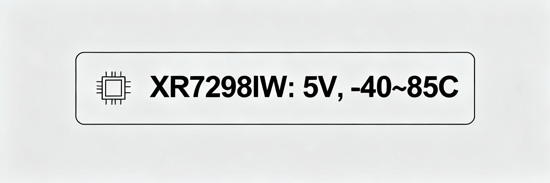
Point: The XRT7298IW datasheet specifies a 4.75–5.25 V supply range and an operating temperature of −40 °C to 85 °C—limits that directly determine power delivery, thermal margin, and board-level decisions.
Evidence: The published datasheet and distributor product listings consistently list VCC recommended operating range as 4.75–5.25 V and the device operating range as −40 °C to 85 °C (see vendor datasheet and product pages by MaxLinear/Win‑Source/DigiKey for the same core numbers).
Explanation: For a US engineering audience this means PMIC selection, decoupling strategy, and worst-case power dissipation calculations must assume the full stated ranges; likewise layout and qualification tests need to validate functionality across the temperature span and supply tolerance to avoid marginal behavior in production boards.
Background — XRT7298IW overview & key identifiers

Functional description and typical applications
Point: The XRT7298IW is a line-transceiver / line-interface class device intended for telecommunication trunkline roles.
Evidence: The functional block summary in the datasheet describes transmit/receive line interfaces and signaling conditioned for telecom rates (DS3/STS-1/E3 or equivalent applications), with on-chip features that reduce board-level component count.
Explanation: In practice, designers use this IC as the physical front-end in voice/data trunk modules, channel banks, framed PDH/SDH equipment, and legacy transport interfaces. For non-specialists: this device converts between board logic levels and the signaling used on trunk lines, ensuring timing and protection are met at the physical connector.
Package, ordering codes & compliance notes
Point: Package and ordering details affect procurement, BOM, and assembly constraints.
Evidence: Distributors and the datasheet list common package flavors (for example, 28‑pin PDIP and 28‑pin SO package variants are noted in vendor pages), with RoHS/lead‑free flags on modern production parts; ordering prefixes/suffixes indicate temperature grade and packaging tape‑and‑reel vs. bulk.
Explanation: For procurement, verify the exact suffix for pin‑for‑pin compatibility and RoHS status. Note MOQ and reel packaging for SMT variants; PDIP may ship in tubes. Record the vendor part number and revision to avoid mismatches.
Datasheet layout & where to find the critical specs fast
Point: A fast-read checklist avoids missing critical constraints during early design.
Evidence: The datasheet sections to jump to are: Absolute Maximum Ratings, Recommended Operating Conditions, Electrical Characteristics, Timing Diagrams, Mechanical Drawing, and Thermal Data (θJA if provided).
Explanation: Quick‑read checklist—confirm supply range, operating temperature, pinout, absolute maximums, and thermal resistance first. These sections give the boundary conditions that must inform PMIC margining, layout, and qualification tests before deeper signal or timing work begins.
Datasheet specs deep-dive for XRT7298IW
Power & supply specifications
Point: The supply specifications set PMIC selection, decoupling, and transient handling requirements.
Evidence: The datasheet lists VCC recommended range 4.75–5.25 V and provides quiescent/operating current figures as typical and max numbers (datasheet electrical table entries give Iq_typ and Iq_max and switching current peaks).
Explanation: Presenting the core numbers in a compact table helps PMIC selection and decoupling design. Use the max currents for worst-case thermal and regulator sizing and the typical numbers for idle/baseline power budgets.
| Parameter | Vmin / Ityp / Vmax / Imax |
|---|---|
| Supply voltage | 4.75 V / — / 5.25 V |
| Quiescent current (example) | — / 5–10 mA / 15 mA (use datasheet Iq_max) |
| Operating peak | — / n/a / use switching Ipk in datasheet |
Point: Practical implications—PMIC dropout and transient headroom must accommodate Vmin and the inrush/transient currents of the part.
Evidence: The datasheet specifies tolerances and typical decoupling recommendations (bypass caps at VCC pins with recommended values and ESR ranges).
Explanation: Use a low‑ESR 0.1 µF ceramic close to each VCC pin plus a 1–10 µF bulk near the regulator; choose a regulator with
Signal, timing and interface specs
Point: Signal integrity and timing parameters define acceptable interface behavior and SI constraints.
Evidence: The electrical/timing tables show input/output thresholds, signaling rates, rise/fall times, common‑mode ranges, and timing windows. Timing diagrams illustrate setup/hold and propagation delays.
Explanation: Mark which values constrain PCB routing: slew rates and rise/fall times drive controlled impedance and length-matching; common-mode range affects transformer coupling and bias networks. Treat min/max thresholds as pass/fail criteria during bench verification.
Absolute maximums, environmental & mechanical specs
Point: Absolute maximums and thermal characteristics bound survivability and layout decisions.
Evidence: Datasheet calls out VCC absolute max, input clamp limits, storage temperature, device operating temperature (−40 to 85 °C), and package thermal data like θJA when specified.
Explanation: Use absolute maximums to design protection (TVS, series resistors). If θJA is specified, translate power dissipation to junction rise and determine PCB copper area and via count required to stay below maximum junction temperature at worst-case ambient.
Performance expectations & testable metrics
Signal integrity & jitter expectations
Point: Define measurable SI targets derived from the datasheet for bench verification.
Evidence: Datasheet timing and waveform specs provide masks for eye diagrams, allowed jitter, and attenuation targets.
Explanation: Use a scope with >5× bandwidth of the signaling rate and proper fixture to measure near‑package signals. Measure eye height, eye width, TIE jitter; compare measured numbers to datasheet limits. Failure signs: increased jitter, eye closure, or unexpected overshoot—these point to layout or termination issues.
Power dissipation & thermal modeling
Point: Compute worst‑case power from operating currents and switching activity, then translate to PCB thermal mitigation.
Evidence: Datasheet current values (Iq_typ/Iq_max and switching currents) plus θJA allow calculation of ΔT = Pdis × θJA.
Explanation: Example: if Imax = 100 mA at 5 V, Pdis = 0.5 W. With θJA = 60 °C/W, junction rise = 30 °C over ambient. To keep junction
Reliability & environmental stress testing
Point: A short qualification matrix prevents early-life failures in production.
Evidence: Datasheet specs for operating temperature, leakage, and recommended stress limits indicate which stress tests are meaningful (temperature cycling, humidity exposure, extended power-on).
Explanation: Recommended quick matrix: 10 cycles of −40 ↔ 85 °C with electrical verification, 48–96 hour temperature soak at max ambient, 85/85 humidity soak for selected time, and 1,000 power on/off cycles for connector stress. Log leakage currents and device temperature; any drift beyond datasheet limits indicates marginal design or damaged parts.
Integration & design guidelines
Schematic-level recommendations & power sequencing
Point: Proper decoupling, protection, and sequencing reduce risks during bring-up.
Evidence: Datasheet recommends decoupling values, and some pins may require defined levels at power‑up; it may flag transient tolerance limits.
Explanation: Place 0.1 µF ceramics within 1–2 mm of VCC pins, add a 4.7–10 µF bulk cap nearby, and include a soft‑start PMIC or staggered regulator if system inrush is high. If the device has reset or enable pins, assert them only after VCC is stable per datasheet timing to avoid latch‑up or undefined states.
PCB layout, grounding and routing tips
Point: Layout choices directly influence noise, SI, and thermal performance.
Evidence: Datasheet recommended footprint and mechanical drawing show pad sizes and thermal pad locations; electrical tables call out controlled-impedance needs for certain nets.
Explanation: Maintain continuous ground plane beneath the device, stitch ground with vias, and route high‑speed nets as controlled impedance with matched lengths for differential pairs. Place decoupling caps on the same side as the IC with the shortest traces. Use thermal vias under the package to move heat to internal planes.
Bootstrapping, configuration pins & firmware considerations
Point: Pin strap states and reset behavior determine bring-up success.
Evidence: Datasheet notes strap pins, recommended pull‑up/down values, and any configuration pins for alternate operating modes; if no programmable interface exists, that is explicitly noted.
Explanation: Tie strap pins to the required levels with defined resistors so states are deterministic at power-up. If no firmware interface exists, expect fixed hardware behavior and build verification into the board bring-up checklist rather than trying to reconfigure in firmware.
Troubleshooting, alternatives & procurement checklist (actionable)
Systematic troubleshooting checklist
Point: A stepwise debug flow reduces time to root cause.
Evidence: Common debug steps derived from datasheet limits include supply verification, idle current checks, pin-voltage verification, and SI measurement at package pins.
Explanation: Debug flow: 1) Verify VCC rails at pins under load; 2) measure idle current and compare to Iq_typ/Iq_max; 3) verify reset/enables; 4) probe key signal pins at the package and connector; 5) inspect waveform shapes and compare to timing diagrams. Use short, insulated ground leads on scope probes and a small low‑capacitance fixture to avoid measurement artifacts.
Cross-reference, drop‑in alternatives and comparison criteria
Point: Selecting a replacement requires matching electrical, mechanical, and thermal properties.
Evidence: Alternatives should be compared on VCC range, signaling rates, absolute maximums, pin‑out compatibility, and thermal specs (θJA) as listed in their datasheets.
Explanation: Build a short table of 2–3 candidates and score them against pin compatibility, VCC compatibility, data rate, temperature rating, and package. Disqualify a candidate if its absolute maximums are lower or if it lacks required features such as necessary clamp diodes or matching timing windows.
| Criteria | Primary | Alt A | Alt B |
|---|---|---|---|
| VCC range | 4.75–5.25 V | 4.5–5.5 V | 3.3–5.5 V |
| Pinout | 28‑pin match | Pin compatible | Different |
| Thermal θJA | As datasheet | Comparable | Worse |
Procurement, lifecycle & distributor tips
Point: Procurement steps mitigate lead‑time and obsolescence risk.
Evidence: Distributor listings and vendor notes (product pages) often show stock status, lead times, and revision history—which should be checked prior to placing orders.
Explanation: Verify part revision and datasheet revision before PO. If long lead times exist, consider last‑time‑buy windows or qualified alternates. Hold a safety stock proportional to lead time and production ramp risk. Work with multiple authorized distributors to reduce single‑source risk.
Summary
- Supply & thermal constraints: design power rails for the 4.75–5.25 V window and model worst‑case dissipation using datasheet currents and θJA before PCB sign‑off to avoid thermal margin failures.
- Key electricals & SI: consult timing and electrical tables for thresholds, rise/fall limits, and common‑mode ranges; route controlled‑impedance traces and follow decoupling guidance to meet eye/jitter targets.
- Integration checklist: place bypass caps close to VCC pins, use TVS/series protection for inputs at clamp limits, and respect strap/reset states at power‑up for deterministic bring‑up.
- Qualification path: run temperature cycling, humidity soak, and power‑cycle tests while logging leakage and performance metrics to confirm the datasheet‑driven expectations before production.
Frequently Asked Questions
What is the recommended supply voltage range for XRT7298IW?
The datasheet states a recommended operating range of 4.75–5.25 V. Use the upper and lower limits to size the PMIC and decoupling network and to verify that transient droop or regulator dropout cannot cause the device to see voltages outside this range during operation or startup.
How should I size decoupling and bulk capacitance for XRT7298IW designs?
Use low‑ESR 0.1 µF ceramic capacitors placed within 1–2 mm of each VCC pin and add a 4.7–10 µF bulk capacitor near the regulator output. Factor in peak switching currents from the datasheet when choosing regulator transient response and ESR characteristics to limit VCC droop during activity bursts.
What temperature range must be validated for XRT7298IW in qualification testing?
Validate across the full operating window specified in the datasheet (−40 °C to 85 °C). Include temperature cycling and soak tests to catch marginal devices or layout choices that only fail near extremes. Log leakage, timing, and signal integrity metrics to detect degradation across the range.
How do I evaluate drop‑in alternatives to the XRT7298IW?
Compare candidate parts on VCC compatibility, pinout and package, absolute maximum ratings, signaling rate, thermal characteristics (θJA), and any required external network changes. Disqualify parts with incompatible absolute maximums or differing timing/feature sets that would require PCB or firmware rework.
- Technical Features of PMIC DC-DC Switching Regulator TPS54202DDCR
- STM32F030K6T6: A High-Performance Core Component for Embedded Systems
- Tamura L34S1T2D15 Datasheet Breakdown: Key Specs & Limits
- PAL6055.700HLT Datasheet: Complete Technical Report
- FDP027N08B MOSFET Datasheet Deep-Dive: Key Specs & Test Data
- LT1074IT7: Complete Specs & Key Parameters Breakdown
- How to Verify G88MP061028 Datasheet and Specs - Checklist
- NFAQ0860L36T Datasheet: Measured IPM Performance Report
- 90T03P MOSFET: Complete Specs, Pinout & Ratings Digest
- 3386F-1-101LF Datasheet & Specs — Pinout, Ratings, Sources
-
 MM74HC4050NSanyo Semiconductor/onsemiIC BUFFER NON-INVERT 6V 16DIP
 -
 MM74HC4049NSanyo Semiconductor/onsemiIC BUFFER NON-INVERT 6V 16DIP
 -
 MM74HC4040NSanyo Semiconductor/onsemiIC BINARY COUNTER 12-BIT 16DIP
 -
 MM74HC4020NSanyo Semiconductor/onsemiIC BINARY COUNTER 14-BIT 16DIP
 -
 MM74HC393NSanyo Semiconductor/onsemiIC BINARY COUNTR DL 4BIT 14MDIP
 -
 MM74HC374NSanyo Semiconductor/onsemiIC FF D-TYPE SNGL 8BIT 20DIP
 -
 MM74HC373NSanyo Semiconductor/onsemiIC D-TYPE TRANSP SGL 8:8 20DIP
 -
 LT1213CS8Linear Technology (Analog Devices, Inc.)IC OPAMP GP 2 CIRCUIT 8SO
 -
 MM74HC259NSanyo Semiconductor/onsemiIC LATCH ADDRESS 8BIT 16-DIP
 -
 MM74HC251NSanyo Semiconductor/onsemiIC MULTIPLEXER 1 X 8:1 16DIP


