-
- Contact Us
12.288MHz SMD Crystal Report: Specs, ESR & Performance
Engineers select a 12.288MHz crystal because 12.288 MHz = 256 × 48 kHz, making it a native clock choice for many audio codecs, PLL references and timing subsystems. This report summarizes typical electrical specs, ESR behavior and measurable performance factors designers should validate before committing to production.
The following sections give practical acceptance thresholds, lab test methods and procurement checklist items that reflect real bench experience and design trade-offs for surface-mount timing devices.
1 — Background: What is a 12.288MHz SMD crystal and where it’s used
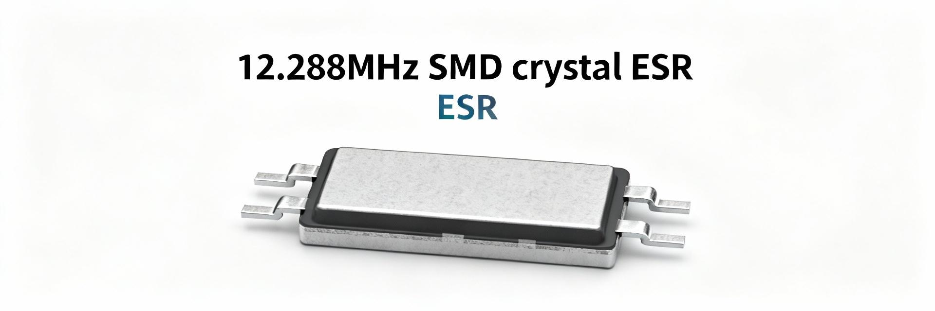
Electrical baseline and mechanical footprints
Point: A 12.288MHz SMD crystal is typically specified as a fundamental-mode, series-resonant device with specified load capacitance. Evidence: typical LC values range 12–18 pF, initial tolerance options ±10 to ±50 ppm, and temp ratings from commercial to industrial. Explanation: pick a footprint (e.g., 3.2×2.5 mm, 2.5×2.0 mm) balancing lower ESR against board space and aging trade-offs.
Typical application domains and why the frequency matters
Point: The 12.288MHz choice aligns directly to audio sample-rate multiples. Evidence: 12.288 MHz = 256 × 48 kHz, so codecs and USB audio interfaces commonly lock to it for low-jitter sample clocks. Explanation: choose 12.288MHz when native audio multiples reduce PLL complexity; otherwise consider nearby clocks when lower jitter or different divider ratios are required.
2 — Key specs: frequency tolerance, stability and load capacitance
Frequency tolerance & temperature stability — what to specify and test
Point: Specify initial tolerance, temperature stability and aging separately. Evidence: typical acceptance: consumer boards tolerate ±30–50 ppm initial and ±100–200 ppm over operating range; industrial designs usually require ±10–20 ppm initial and tighter temp stability. Explanation: tighter tolerance reduces in-system calibration effort but increases part cost and procurement constraints.
Load capacitance and drive level impacts
Point: Load capacitance and drive level both shift operating frequency and influence aging. Evidence: a mismatch of 2–4 pF shifts frequency by parts-per-million; high drive (>100 μW typical spec limits) accelerates aging and can change motional parameters. Explanation: record specified CL, recommended series resistor and maximum drive level when documenting BOM acceptance criteria.
3 — ESR & performance: ranges, effects on oscillator behavior and phase noise
Typical ESR ranges for SMD crystal packages and why ESR matters
Point: ESR directly affects oscillator startup and required amplifier loop gain. Evidence: typical ESR ranges vary with package: mid-size 3.2×2.5 mm parts often show 30–100 Ω; very small 2.0×1.6 mm parts can exceed 150–300 Ω. Explanation: designers must inspect datasheet test data for ESR; a high ESR SMD crystal may need a higher-gain oscillator or different topology to start reliably.
ESR vs oscillator topology: push-pull, Pierce, CMOS oscillator ICs
Point: ESR interacts with circuit topology and feedback network. Evidence: Pierce oscillators tolerate moderate ESR if amplifier loop gain is sufficient; push-pull or buffered CMOS oscillators may require lower ESR or added negative resistance. Explanation: when long startup or unstable amplitude appears, log ESR, adjust feedback resistors, add series resistor or select an oscillator IC optimized for high-ESR crystals.
4 — Measurement & test methods: how to characterize a 12.288MHz crystal
Recommended lab setups and instruments
Point: Use the right tools and fixtures to get repeatable motional parameters. Evidence: typical bench setup includes an LCR meter for motional C1/Lm/Rm, a spectrum analyzer or VNA for phase noise and frequency, plus an oscillator evaluation board to measure startup and drive. Explanation: log test conditions—temperature, supply, load caps and fixture parasitics—to make results actionable for procurement and design revisions.
How to interpret test results and convert to design actions
Point: Translate raw measurements into pass/fail and BOM notes. Evidence: reject lots when ESR or motional C1 deviates more than supplier spec or when measured aging exceeds expected ppm/year. Explanation: typical pass thresholds: ESR within datasheet max, frequency within initial tolerance at 25°C with specified CL, and startup time under design-target (e.g.,
5 — Design considerations: PCB layout, footprint and reliability for SMD crystals
PCB layout and footprint best practices
Point: Layout determines oscillator immunity and measured performance. Evidence: keep traces between crystal pads and amplifier pins as short as possible, avoid ground pours between pads, place ground vias near pads, and keep the oscillator IC within a few mm. Explanation: good pad design and solder fillet control reduce parasitics that otherwise increase effective ESR and degrade phase noise.
Environmental & reliability factors to call out in specs
Point: Assembly and environment affect long-term stability. Evidence: specify soldering profiles, storage humidity limits, and shock/vibration requirements; small SMD packages are more prone to mechanical detuning after thermal cycling. Explanation: include reflow limits and handling notes in BOM to avoid latent frequency shifts or cristallographic damage during assembly.
6 — Procurement, validation checklist & troubleshooting quick-guide
Pre-order spec checklist for sourcing teams
Point: Require complete, testable specs before purchase. Evidence: mandate supplier data: frequency (12.288MHz), initial tolerance (ppm), stability over temp, max ESR, CL, package drawing, test conditions, lot traceability and sample availability. Explanation: including the phrase 12.288MHz crystal in the procurement spec ensures alignment across engineering and sourcing and reduces ambiguity in test-condition interpretations.
Onboard validation steps and common failure modes to test
Point: Validate parts on bench and in-system before volume buy. Evidence: a minimal flow: bench motional parameter check → oscillator board startup → in-system startup under defined supply and temp → phase-noise spot check if required → thermal cycling. Explanation: common failures include high ESR causing no-start, frequency pull from wrong CL, and soldering damage; record measured ESR, startup time and frequency offset for failure analysis.
Summary
For audio and timing-critical designs the 12.288MHz crystal choice must be validated for ESR, load capacitance and measured stability under real operating conditions before volume buys. Use the procurement and validation checklist above to reduce field failures and ensure oscillator reliability; document measured ESR, CL and startup behavior alongside lot traceability.
Key Summary
- Validate ESR and motional parameters: ensure measured ESR is within datasheet max and startup time meets system requirements to avoid no-start scenarios.
- Specify load capacitance and drive limits: record CL, series resistor and max drive level to control frequency pull and aging in-system.
- Follow PCB and assembly best practices: short traces, consistent solder fillets and thermal profile control reduce parasitics and long-term drift.
Frequently Asked Questions
How tight should initial tolerance be for a 12.288MHz timing clock?
Answer: For consumer audio, ±30–50 ppm initial tolerance is common; industrial or precision audio often requires ±10–20 ppm. Select tolerance based on whether software calibration or PLL discipline will correct residual offset; tighter tolerances reduce system-level calibration burden but increase part cost and procurement constraints.
What ESR limit should be required when specifying a 12.288MHz SMD crystal?
Answer: Require the supplier’s datasheet max ESR and insist on measured sample results; typical mid-size SMD parts show 30–100 Ω while very small parts may exceed 150 Ω. Use oscillator evaluation to confirm startup and adjust component selection if ESR impairs loop gain.
What are quick in-system tests to detect crystal-related failures?
Answer: Run bench motional checks, power-up startup timing, in-system frequency offset under nominal load caps, and a short thermal cycle. Log ESR, startup time and frequency shift; failure patterns (no-start, large pull with CL changes, sudden drift) point to ESR, solder damage or incorrect CL choice.
- Technical Features of PMIC DC-DC Switching Regulator TPS54202DDCR
- STM32F030K6T6: A High-Performance Core Component for Embedded Systems
- Tamura L34S1T2D15 Datasheet Breakdown: Key Specs & Limits
- PAL6055.700HLT Datasheet: Complete Technical Report
- FDP027N08B MOSFET Datasheet Deep-Dive: Key Specs & Test Data
- LT1074IT7: Complete Specs & Key Parameters Breakdown
- How to Verify G88MP061028 Datasheet and Specs - Checklist
- NFAQ0860L36T Datasheet: Measured IPM Performance Report
- 90T03P MOSFET: Complete Specs, Pinout & Ratings Digest
- 3386F-1-101LF Datasheet & Specs — Pinout, Ratings, Sources
-
 MM74HC4050NSanyo Semiconductor/onsemiIC BUFFER NON-INVERT 6V 16DIP
 -
 MM74HC4049NSanyo Semiconductor/onsemiIC BUFFER NON-INVERT 6V 16DIP
 -
 MM74HC4040NSanyo Semiconductor/onsemiIC BINARY COUNTER 12-BIT 16DIP
 -
 MM74HC4020NSanyo Semiconductor/onsemiIC BINARY COUNTER 14-BIT 16DIP
 -
 MM74HC393NSanyo Semiconductor/onsemiIC BINARY COUNTR DL 4BIT 14MDIP
 -
 MM74HC374NSanyo Semiconductor/onsemiIC FF D-TYPE SNGL 8BIT 20DIP
 -
 MM74HC373NSanyo Semiconductor/onsemiIC D-TYPE TRANSP SGL 8:8 20DIP
 -
 LT1213CS8Linear Technology (Analog Devices, Inc.)IC OPAMP GP 2 CIRCUIT 8SO
 -
 MM74HC259NSanyo Semiconductor/onsemiIC LATCH ADDRESS 8BIT 16-DIP
 -
 MM74HC251NSanyo Semiconductor/onsemiIC MULTIPLEXER 1 X 8:1 16DIP

