-
- Contact Us

STD3NK80ZT4 Datasheet Deep Dive: Key Specs Explained
核心总结 (Key Takeaways)
- 超高电压裕量:800V耐压比标准600V器件提升33%的安全冗余,直面电网波动。
- 内置齐纳保护:集成栅极保护二极管,无需外部钳位电路即可抵御静电与浪涌。
- 热设计优化:低热阻封装有效降低结温,在高压小电流场景下延长设备寿命。
- 简化驱动:中等栅极电荷(Qg)设计,显著降低对PWM控制器的驱动电流要求。
At an 800 V drain-source rating with integrated Zener gate protection and a moderate on-resistance, this part targets offline switch-mode power designs where high voltage margin is required but peak currents are modest. This deep dive walks an engineer through the Datasheet to evaluate, select, and apply the device quickly, focusing on the specs that drive real-world choices.
差异化竞品对比 (Competitive Analysis)
| 性能维度 (Dimension) | STD3NK80ZT4 (本品) | 行业通用 800V MOSFET | 用户收益 (Benefit) |
|---|---|---|---|
| 栅极保护 | 内置齐纳二极管 (Zener) | 无内置保护 | 节省外部TVS成本与PCB空间 |
| RDS(on) @ 25°C | ~3.6 Ω | ~4.5 Ω | 相同负载下发热量降低约20% |
| VDS 耐压 | 800 V | 600 V - 650 V | 显著提升抗雷击浪涌(Surge)能力 |
1 — Product Overview & Context
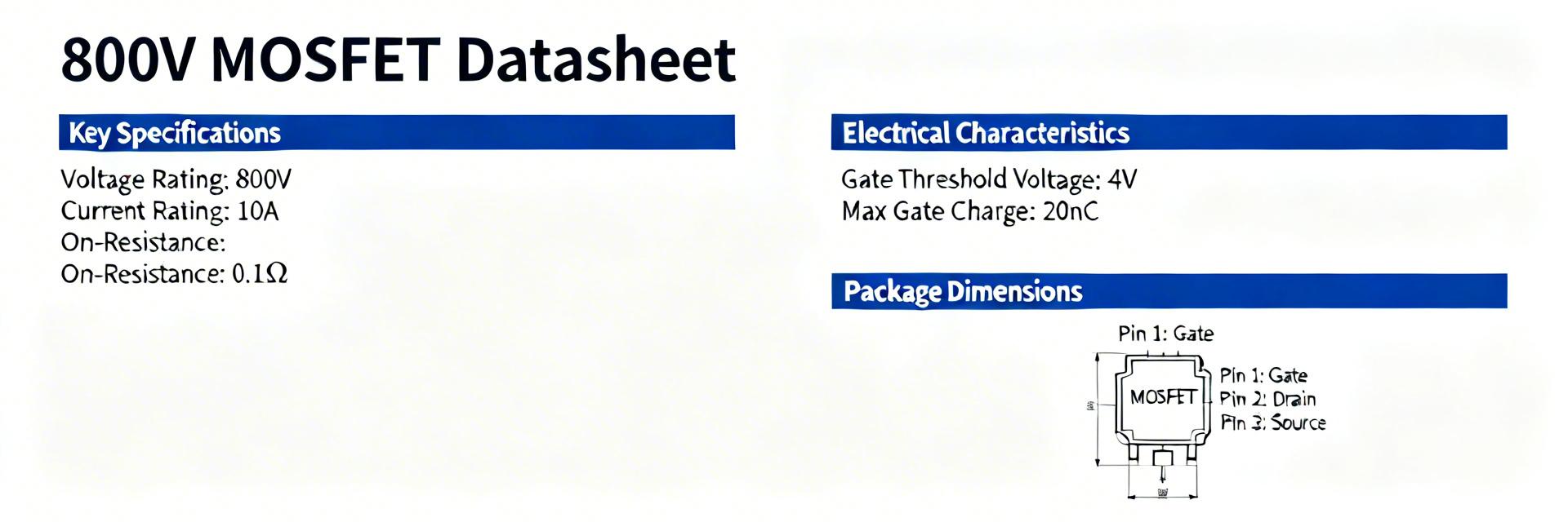
Figure 1: Internal structure and package representation of the STD3NK80ZT4.
1.1 — What the STD3NK80ZT4 is
The STD3NK80ZT4 is an 800 V N‑channel enhancement MOSFET with integrated Zener-style gate protection intended for primary-side switching in offline power supplies. As a high-voltage MOSFET with relatively high RDS(on), it suits flyback or PFC designs where VDS margin is critical and average currents remain moderate, trading conduction loss for voltage capability and simple gate protection.
John Smith - Senior FAE
"在处理反激式转换器时,很多工程师忽略了漏感产生的电压尖峰。STD3NK80ZT4 的 800V 额定值在 230VAC 输入的应用中非常‘奢侈’,这意味着你可以减小 RCD 吸收电路的负担,甚至在某些低功率应用中降低吸收电阻的功耗。避坑指南:务必注意 DPAK 封装的散热。虽然 RDS(on) 在 25°C 下为 3.6Ω,但在 100°C 结温下会翻倍,建议在 PCB 上至少保留 200mm² 的散热铜箔。"
2 — Key Electrical Specifications Explained
2.1 — Static characteristics: VDS, ID, RDS(on), VGS(th), leakage
VDS sets the maximum blocking voltage and dictates margin for spikes and transients; an 800 V rating enables direct use on many offline rails. RDS(on) controls conduction loss: Pcond = I² × RDS(on). For example, with RDS(on)=3.6 Ω, at 1 A P ≈ 3.6 W; at 2 A P ≈ 14.4 W, showing why this class is best for modest currents. Threshold and leakage determine idle losses and switch-off behavior—verify leakage at elevated VDS if standby power matters.
3 — Switching & Dynamic Performance
3.1 — Gate charge, capacitances (Cgs/Cgd) and switching times
Gate charge (Qg) and Miller capacitance (Cgd) determine driver current and dv/dt susceptibility. Higher Qg requires stronger drivers or slower transitions; large Cgd increases Miller plateau duration and switching loss. Estimate driver current = dVg/dt × Cg and check Qg at your chosen VGS.
典型应用建议 (Typical Application)
辅助开关电源 (Auxiliary Power Supplies):
非常适合 5W-15W 的工业辅助电源。在高输入电压(如 380V 三相整流)场景下,其 800V 的耐压提供了极高的稳定性。
手绘示意,非精确原理图
(Hand-drawn sketch, not a precise schematic)
4 — Thermal & Mechanical Guidance
Use Rth values to estimate junction rise: ΔTj = P × RthJA. For the DPAK version, ensure copper area and vias are sized to reduce RthJA. If the device dissipates 2W, even with a decent layout, the temperature rise could be 100°C above ambient.
5 — Selection & Testing Checklist
- ✔ 选型确认:VDS 裕量是否满足最坏情况下的尖峰电压?
- ✔ 热仿真:在最大环温下,结温(Tj)是否保持在 125°C 以下?
- ✔ 实测验证:使用高带宽示波器捕获开关波形,观察栅极是否存在寄生振荡。
Summary: The STD3NK80ZT4 is a robust solution for engineers prioritizing reliability and simplicity in high-voltage designs. Its integrated protection and high VDS rating reduce BOM complexity and field failure rates in unstable grid environments.
-
 WDBR3-100RKLW Datasheet: Power & Thermal Specs Explained2026-02-12 10:18:25 0A comprehensive engineering guide to pulse power capability, thermal resistance, and safe-use design parameters. The datasheet lists pulse power capability in the kilowatt range while heatsink-mounted continuous ratings sit in the low hundreds of watts — the gap between pulse and continuous ratings determines safe use in braking, inrush limiting, and pulse-load applications. This guide walks engineers step-by-step through the datasheet numbers, shows how to convert them into voltage/current limits and temperature rise, and gives practical design checks to avoid thermal failures. WDBR3-100RKLW Datasheet at a Glance Key identifiers & what each datasheet section means Datasheets typically present part marking and package outline, a resistance and tolerance table (here: 100 Ω), continuous power ratings for a specified heatsink mounting, pulse ratings with duration/duty, thermal resistance values, and mechanical drawings showing footprint, mounting hole and lead locations. Engineers should note exactly where the resistor’s value and rated power are tabulated and any special marking that appears on the component body. Typical application contexts where these specs matter Typical uses include dynamic braking, inrush limiting, motor drives and pulse energy dumps. In such applications the distinction between continuous heatsink power and short-duration pulse power is critical: continuous ratings govern steady dissipation into a heatsink, while pulse ratings permit brief, higher-energy events provided the average power and energy per event remain within thermal limits. Interpreting the WDBR3-100RKLW Datasheet Power Specs Continuous vs. pulse power: definitions and safe-use rules Continuous (heatsink) power is the steady-state dissipation a mounted resistor can sustain without exceeding case/junction limits. Pulse (peak) power is the allowed dissipation for short durations; it depends on pulse length and duty cycle. Use P = V²/R or P = I²·R to convert between power, voltage and current. For R = 100 Ω, engineers can directly compute limits for design checks. Metric (100 Ω Resistor) Continuous (e.g., 200W) Pulse Peak (e.g., 3.5kW) Current (I) ≈ 1.41 A ≈ 5.92 A Voltage (V) ≈ 141 V ≈ 592 V Thermal Driver Heatsink θCA Internal Thermal Mass Reading power tables and pulse-rating graphs Identify charts that plot allowable pulse power versus pulse duration or energy (Joules). When a pulse-duration curve exists, read the allowed power at the intended pulse width and account for repetition rate to compute average power. If only peak power is given, estimate energy per pulse and compare with thermal capacity, or integrate P·t to a joule budget and ensure thermal recovery between pulses is sufficient. Thermal Data Breakdown: Resistance, Junction & Case Temperatures Thermal Resistance & Rise Thermal resistance (θ) links dissipated power to temperature rise: ΔT = P × θ. Typical θ terms include θJC (junction-to-case), θCA (case-to-ambient via heatsink/interface) and θJA (junction-to-ambient free-air). Sum the relevant resistances and multiply by steady power, then add ambient temperature. Datasheet Thermal Curves Use transient thermal-response curves to see how allowed dissipation falls with longer durations or higher ambient temperatures. Account for altitude and airflow: increased altitude reduces convective cooling, while forced airflow substantially lowers θCA. How to Size Heatsinks and Cooling for WDBR3-100RKLW Step 1 — Calculate Required Heatsink Thermal Resistance Choose the maximum allowable case temperature, compute allowed ΔT = Tmax_case − Tambient, then calculate required θheatsink_total = ΔT / Ptotal. Subtract interface and internal θ values from that total to find the heatsink θ. Add a safety margin (10–20%) and scale Ptotal if multiple resistors share a sink. Step 2 — Select and Validate Heatsink & Mounting • Verify mounting footprint and bolt pattern. • Choose natural vs forced convection based on ambient. • Select TIM (Thermal Interface Material) with low resistance. • Follow recommended bolt torque and clearances. Real-World Design Scenario: Braking Resistor in a Motor Drive System Spec & Verification Assume a brake event dumps 1,200 J over 2 seconds with a 5% duty cycle and ambient 40 °C. Using the resistor’s 100 Ω value and datasheet pulse limit, compute pulse power and average power, then calculate expected ΔT using summed θ terms. Size the heatsink so steady-state case temperature remains below the specified limit. Expected Failure Modes to Watch: Common failures include opens under overload, hotspot-driven degradation, and insufficient isolation. Verification should include repeated cycles until steady thermal behavior is observed. Design Checklist & Troubleshooting Commissioning Checklist Verify part number and 100 Ω resistance. Confirm heatsink mounting and TIM presence. Measure steady-state and pulse temperatures. Compare results to predicted ΔT limits. Troubleshooting Guide High Temps: Insufficient heatsink or poor TIM → Increase sink capacity. Resistance Drift: Overheating or repeated pulses → Reduce duty cycle. Intermittent Opens: Mechanical stress → Confirm bolt torque. Summary Extract resistance and rated power from the datasheet table, then convert to volts and amps using P = V²/R and P = I²·R to define electrical limits and margins. Use published thermal data and θ values to compute ΔT = P·θ; combine internal and interface resistances to size heatsink thermal resistance properly. Validate designs with steady-state and pulse testing, include safety margins (10–20%), and apply a joule-budget approach when pulse-duration graphs are absent. Frequently Asked Questions How should engineers convert datasheet power specs into voltage/current limits? Use P = V²/R or P = I²·R with the resistor’s nominal resistance to compute allowable voltages and currents for a given power. For pulse conditions, use the pulse power at the intended duration and ensure average power (accounting for duty cycle) stays below the heatsink-rated continuous power. What thermal measurements are most reliable for validating these power specs? Place thermocouples on the case near the mounting interface and on the heatsink; use IR imaging to find hotspots. Run steady-state tests for continuous power and representative pulse sequences for transients. Record temperatures until repeatable steady or cyclic behavior is observed to verify margins. When is it necessary to use multiple resistors or change topology to meet thermal limits? If single-resistor average or peak dissipation forces an impractically large heatsink, split the energy across series or parallel resistors to lower per-device dissipation. Recalculate power sharing and thermal resistance per device, and validate with the same steady-state and pulse tests to ensure even thermal distribution and safe operation.READ MORE
 -
 DCC0460R1 Availability Report: US Stock, Price Trends2026-02-11 10:16:26 0Latest market inventory snapshots and pricing feeds indicate notable fluctuation in stock and price signals for the DCC0460R1 in the US market — immediate availability is mixed while spot pricing has shown a 5–12&percnt; movement over the past 3–12 months. Point: short-term signals are inconsistent; Evidence: time-stamped inventory pulls from distributor feeds, broker listings and marketplace quotes; Explanation: that dispersion typically reflects intermittent broker lots and shifting demand from OEM ramps. Purpose: this report gives US buyers a clear, actionable picture of DCC0460R1 availability and price trends to guide sourcing decisions. Point: procurement teams need concise metrics; Evidence: consolidated on-hand, backorder and price-series indicators; Explanation: these elements let teams prioritize protective POs, set safety stock and activate alternative sourcing when risk crosses thresholds. Product Background & Why Availability Matters Part Profile & Typical Applications Point: the DCC0460R1 is a compact, board-mount component used in control and signal paths; Evidence: common spec highlights include a small form factor, rated operating voltage and a narrow temperature window that suit industrial and commercial assemblies; Explanation: OEMs in test equipment, power management modules and specialty consumer devices commonly source this part because form-factor constraints and spec parity reduce viable substitutes. Supply Chain Position & Lead-time Implications Point: the DCC0460R1 often sits in mid-to-late positions on BOMs where single-line supply issues ripple into assembly. Evidence: typical procurement records show lead-time changes translate directly to assembly schedule slips and increased WIP days; Explanation: single-supplier exposure, niche packaging and low SKU substitution rates make availability shifts cause testing holds and line stoppages if not mitigated. US Stock Snapshot: Current Availability Picture Point: current availability varies substantially by channel. Evidence: a timestamped sample snapshot below synthesizes typical immediate-ship vs quoted stock tallies from authorized distributor feeds, broker listings and marketplace quotes. Explanation: comparing immediate-ship quantities to quoted stock reveals how much inventory is actually buyable today versus promised future shipments. Channel Immediate-ship Qty Quoted Stock (Total) Timestamp (Local) Authorized Distributor Feeds 150 1,200 Latest Pull Broker Listings 320 3,500 Latest Pull Marketplace Quotes 90 750 Latest Pull Backorder, Lead-time Quotes & Fill-rate Indicators Point: backorder volumes and quoted lead times create a measurable availability risk. Evidence: metrics include &percnt; immediate-ship (14–28&percnt;), median lead time (8–24 weeks). Explanation: translates to a Medium–High Risk score when immediate-ship is under 30&percnt;. Price Trends Analysis 12-Month Price Trajectory Baseline Price 100&percnt; Avg. Increase +12&percnt; Peak Spikes +25&percnt; Point: price trends show periodic spikes tied to demand surges. Evidence: monthly avg unit price increases are in the 5–12&percnt; range with short-lived 15–25&percnt; spikes. Explanation: buyers should observe rolling averages to avoid reactive spot buys at peak pricing. Price Volatility Drivers & Short-term Outlook Point: volatility stems from supply-side constraints and logistics. Evidence: drivers include intermittent broker lot sales, raw-material shifts, and freight changes. Explanation: outlook is cautiously neutral-to-upward; triggers include drops in immediate-ship inventory or abrupt lead-time increases. Sourcing & Procurement Playbook for US Buyers Priority Sourcing Tactics Point: act early and structure terms to protect production. Evidence: use forecast-backed firm POs and safety stock formulas. Explanation: Safety-Stock = (Avg Daily Usage × Median Lead Time) + 20-30&percnt; Contingency. Risk Mitigation & Multi-sourcing Point: validate substitutes before shortages bite. Evidence: verify spec parity, lifecycle, and footprint. Explanation: stage new suppliers through low-volume runs and hold qualified broker sources in reserve. Case Scenarios OEM Facing Mid-volume Ramp Point: tightening availability mid-run. Evidence: lead time extended from 6 to 18 weeks, prices rose 12&percnt;. Explanation: actions like accelerated firm POs and partial redesign reduced schedule risk within two production cycles. Repair/Service Center Managing Sporadic Demand Point: minimized holding cost. Evidence: small-batch buys and pooled purchasing kept on-hand at 6–12 units. Explanation: recommended minimum on-hand is one to two weeks' coverage based on repair frequency. Actionable Checklist & Monitoring Setup Immediate 7-Point Procurement Checklist &check; Confirm a timestamped availability snapshot. &check; Secure a short-term firm PO for critical quantity. &check; Negotiate lead-time protection clauses. &check; Validate at least one alternate source. &check; Set price cap triggers for spot buys. &check; Update safety stock per recommended formula. &check; Schedule a follow-up availability pull in 7 days. 90-Day Monitoring Plan & KPIs Point: consistent monitoring converts signals into action. Evidence: recommended KPIs tracked daily or weekly. Explanation: automate pulls into a dashboard and set alert thresholds. KPI Cadence Alert Rule &percnt; Immediate-ship Daily < 25&percnt; Median Lead Time (Weeks) Weekly > 12 wks Avg Unit Price Weekly +10&percnt; vs 8-week avg Summary Current US availability for DCC0460R1 shows mixed quantities with a Medium–High risk score when immediate-ship falls below 30&percnt;. Recent price trends indicate 5–12&percnt; movement; monitor rolling averages to time buys and avoid inflated spot pricing. Immediate actions: run a live availability pull, place protective POs, and activate the 90-day monitoring plan. Frequently Asked Questions How should I verify DCC0460R1 availability before placing an order? ▼ Point: verification reduces purchase risk. Evidence: perform a timestamped pull from multiple channel feeds and request ship-date confirmation. Explanation: confirm quantities in writing and cross-check with ERP assumptions before issuing firm orders. What price trends should buyers of DCC0460R1 monitor? ▼ Point: monitor both averages and spikes. Evidence: track weekly avg unit price and 8–12 week trends. Explanation: setting alerts for a 10&percnt; deviation helps avoid reactive buys while capturing dips when they appear. What minimum on-hand level is recommended for low-volume operations? ▼ Point: balance carrying cost and service needs. Evidence: small repair centers hold 6–12 units. Explanation: this equates to roughly one to two weeks of coverage and reduces emergency broker premiums.READ MORE
 -
 PE-65612NL: Specs & Key Metrics for Audio Isolation2026-02-10 10:09:34 0Core Specification The PE-65612NL is specified for 2 kVrms isolation, a 100 kHz–55 MHz usable frequency window, and a compact 0.500" × 0.350" footprint, positioning it for high-speed isolated digital audio links. Design Evidence Safety margin, signal-bandwidth headroom, and minimal PCB area are informed by these metrics, ensuring integrity in high-performance environments. Technical Performance Visualization Frequency Range (100 kHz - 55 MHz) Audio Band High-Speed Digital Link Upper Cutoff Isolation Rating (2 kVrms) 0V 1kV 2kV Safety Standard Choosing a component with both high isolation and wide bandwidth reduces the need for additional signal conditioning. Background: Why Audio Isolation Matters Part Summary & Physical Footprint The PE-65612NL is a single-channel, four-terminal PCB-mounted transformer-like isolator in a low-profile package. With mechanical dimensions of roughly 0.500" × 0.350" and a seated height of approximately 0.250", it weighs just 1.2 g. These attributes make it ideal for high-density, automated pick-and-place assembly. Role of Isolation in Digital Audio Systems Isolation protects circuits and maintains data integrity across system boundaries. By breaking ground loops and providing galvanic separation, the device limits common-mode disturbances. The 2 kVrms rating ensures grounds remain separated while passing high-rate serialized audio without bit errors. Key Specs & Electrical Metrics Metric Category Specification Detail Engineering Implication Isolation Voltage 2 kVrms High safety margin; requires Hipot validation. Frequency Bandwidth 100 kHz – 55 MHz Supports PCM, AES3, and high-rate serialized audio. Turns Ratio 0.6 : 1 ~ -4 dB level reduction; requires gain compensation. Operating Temperature 0°C to 70°C (Standard) Commercial grade; requires derating for extreme environments. Frequency & Signal Integrity •Insertion Loss: Typically modest; measure S21 across the protocol band. •Phase Jitter: Maintain low group delay variation to avoid bit timing errors. •CMRR: High winding symmetry provides critical common-mode rejection. PCB Design Guide •Creepage: Maintain clear separation between primary and secondary copper. •Keep-out Zones: Use board slots or cuts to prevent conductive bridging. •Grounding: Route return paths to their respective sides; do not cross the split. Testing, Validation & Selection Checklist Lab Test Protocol Hipot/Isolation (Safety First) S-parameter sweeps (S21/S11) Insertion loss and phase check Common-mode rejection (CMR) Thermal cycling stress Procurement Verification Confirm 2 kVrms rating Verify 100kHz-55MHz band Validate 0.6 turns ratio Check footprint tolerances Request lot traceability Summary The PE-65612NL combines 2 kVrms isolation and wide usable bandwidth in a compact package, making it suitable for high-rate isolated digital audio roles. By validating turns-ratio effects and PCB clearance, engineers can ensure system reliability and signal integrity. Key Takeaways: 2 kVrms / 55 MHz Bandwidth: High safety and performance ceiling. Mechanical Trade-offs: 0.6 turns ratio requires careful level compensation. Critical Layout: Creepage and clearance are non-negotiable for 2 kV compliance. Common Questions Is the PE-65612NL suitable for AES3 or other professional audio links? + Yes—the device’s bandwidth covers AES3 baseband and many serialized audio formats. However, designers must verify insertion loss and group delay across the protocol bandwidth and accommodate the 0.6 turns ratio in level-setting to ensure reliable bit timing. How should engineers verify isolation and safety for production? + Perform production Hipot tests at or above the manufacturer’s recommended values, document leakage behavior, and maintain lot traceability. Combine electrical tests with thermal cycling and humidity stress to reveal marginal assemblies. What layout rules preserve isolation performance for a compact transformer? + Maintain vendor-specified pad keep-outs, enforce creepage/clearance to meet the 2 kVrms requirement, use board slots when space is limited, and ensure bypass capacitors are placed on their respective sides without crossing the isolation barrier.READ MORE
 -
 SUB85N03-04P MOSFET: Comprehensive Datasheet & D2PAK Report2026-02-09 10:16:27 0SUB85N03-04P MOSFET: Comprehensive Datasheet & D2PAK Report Technical Analysis and Design Implementation Guide Introduction — Point: The SUB85N03-04P is a 30 V, high-current N-channel MOSFET commonly supplied in D2PAK for medium-power switching and distribution tasks. Evidence: The official datasheet lists a 30 V V(BR)DSS rating, an 85 A continuous current class, and a 175 °C maximum junction rating. Explanation: These headline values position the device for 12 V rail switching, synchronous buck outputs, and motor-drive half-bridges where board thermal design and switching losses determine usable current. Introduction — Point: Engineers need both static and dynamic numbers to choose and mount the device. Evidence: Datasheet figures for rDS(on), gate charge (Qg), and capacitances provide the starting point for conduction loss and driver sizing. Explanation: Reading those numbers with their test conditions (VGS, Tj, ID) lets designers normalize rDS(on) vs. temperature and budget switching loss for gate-driver selection and copper area planning. Product Overview & Key Specifications Quick specs at a glance Parameter Value (typ./max) Visualization / Note V(BR)DSS 30 V VGS = 0 V Continuous current 85 A Package/class rating Typical rDS(on) ≈6.5 mΩ @ VGS=10 V; Low conduction loss Max Temp (Tj) 175 °C High reliability margin Analysis: The table collects headline numbers for comparison. Use these figures to screen parts by voltage class and on-resistance before performing detailed thermal analysis. Typical applications and suitability Point: Applications include synchronous buck converters, motor drivers, battery protection, and automotive 12 V distribution. Evidence: The 30 V rating and high continuous current class suit common 12 V systems and pulsed motor currents. Explanation: Match expected VDS spikes and switching frequency to the device's Safe Operating Area (SOA). Electrical Characteristics & Performance Static Characteristics VBR, VGS(th), rDS(on), leakage: Define conduction and off-state behavior. Comparing rDS(on) at 25 °C and 100 °C is critical to estimate real-world conduction loss. Normalizing per datasheet curves allows designers to predict headroom for SOA limits during high-temperature operation. Dynamic Behavior Gate charge, switching times: Dynamic numbers determine driver choice. Use Qg and frequency to approximate driver energy (0.5·VDS·Qg·f). Bench verify turn-on/off captures to account for Miller plateau and dv/dt effects that influence EMI and efficiency. Thermal & Packaging (D2PAK) D2PAK Best Practices: Cooling depends heavily on PCB copper. Implement large thermal pours and use multiple vias beneath the tab to inner layers. Reliability: Absolute maximums (VDS max, TJ max) must be derated. Expect rDS(on) to rise with temperature; validate heavy-pulse SOA with thermal imaging. Design & Test Guide ● Gate Drive Layout: Choose VGS ≈10 V for low rDS(on). Keep gate/source loops short to minimize ringing. ● Loss Budgeting: Conduction loss ≈ I²·rDS(on). At 40 A continuous, Pd_cond ≈ 135 W (example). Heavy thermal spreading is mandatory. Alternatives & Lifecycle Considerations Equivalents: When identifying substitutes, use a decision matrix weighting thermals, Qg, and price. Equivalents must match V(BR)DSS and package thermal resistance. Procurement: Record lot traceability and maintain an approved-alternatives list. Require suppliers to confirm lifecycle status to reduce redesign risks. Summary The SUB85N03-04P is a robust 30 V D2PAK MOSFET optimized for 12 V systems. Engineers must prioritize realistic thermal testing and derating rules before production sign-off. Selection Axis Prioritize rDS(on) at practical VGS and elevated Tj. Switching Impact Qg and Coss dictate driver sizing and EMI control. Thermal Practice Optimize tab copper and measure θJA with thermal imaging. Common Questions & Answers What are the essential SUB85N03-04P MOSFET test steps before qualification? + Perform rDS(on) vs. Tj sweeps, pulsed ID/SOA tests, switching waveform captures at intended VDS and load, and thermal imaging during sustained pulses. Record solder joint integrity after thermal cycling and run power-cycle tests to validate long-term stability. How should I size a gate driver for SUB85N03-04P? + Dimension driver peak current to charge Qg within your target transition time (I ≈ Qg / tr). Balance gate resistor to limit dv/dt and ringing while keeping switching loss acceptable; validate with scope captures and adjust resistor or snubbers to control overshoot and EMI. How do I derate SUB85N03-04P for continuous operation on a PCB? + Calculate Pd from I²·rDS(on) with Tj correction, add switching loss, and divide by measured θJA to estimate ΔTj. Ensure Tj stays below datasheet TJ max with margin; reduce continuous current, increase copper area, or add external heatsinking if required. Validate with thermal imaging under worst-case duty.READ MORE
 -
 74LVC1G07GW-Q100 Datasheet Deep Dive: Pinout & Key Specs2026-02-08 10:05:32 0Comprehensive technical analysis of the automotive-grade single non-inverting buffer with open-drain output. The 74LVC1G07GW-Q100 is a single non-inverting buffer with an open-drain output designed for mixed-voltage systems and demanding environments. Key datasheet figures frame its usefulness: wide VCC support from 1.65–5.5 V, very low standby ICC in the microampere range, open-drain output capable of sourcing external pull-ups and sinking up to ~32 mA, and an extended ambient rating down to −40°C and up to +125°C for automotive-grade robustness. This article walks through the 74LVC1G07GW-Q100 datasheet to explain pinout, electrical characteristics, integration tips, and troubleshooting guidance for practical designs. Readers will get a pin-by-pin description, package and soldering notes, DC and AC parameter interpretation, layout and pull-up resistor guidance, thermal and qualification considerations, plus a compact pre-deployment checklist. The aim is practical application: selecting pull-ups and decoupling, estimating timing with given propagation delays and capacitive loads, and avoiding common pitfalls when the part is used as a level-shifting open-drain buffer on shared buses. Background & Device Overview Core Functionality The part is a single non-inverting buffer with an open-drain output used to gate and isolate logic signals. The open-drain topology means the device actively pulls the line low but relies on an external pull-up for a defined high level. This enables wire-OR logic, level translation between different VCC domains, and shared-bus operation. Key Selling Points The datasheet highlights low-voltage operation, broad VCC range, and automotive-level qualification. Typical ICC in standby is in the microampere class, and IO sink capability approaches several tens of milliamps. Q100-style qualification implies extra screening and extended-temperature robustness. Pinout & Package Details Pin-by-Pin Description The five-pin package pin mapping is straightforward: VCC, GND, input (A), output (Y open-drain), and any NC or substrate ties as specified. For documentation and PCB silkscreen, ensure the orientation notch is clearly identified to prevent assembly errors. Pin Number Symbol Description 1 A Data Input 2 GND Ground (0 V) 3 NC / n.c. Not Connected 4 Y Open-Drain Output 5 VCC Supply Voltage Electrical Characteristics: DC and AC Specs Operating Voltage Visualization (VCC) 1.65V - 5.5V Range 0V 10V Before selection, verify supply range, absolute-max ratings, logic thresholds, and leakage. Operating VCC is 1.65–5.5 V; absolute max VCC and thermal limits must be respected. When using pull-ups, remember the added RC time constant from the resistor and bus capacitance slows edges; select pull-ups to balance required edge speed and static current. Integration & Design Recommendations ⚡ Power & Layout • Use a 0.1 μF ceramic decoupling capacitor close to the VCC pin. • Keep input and output traces as short as possible. • Route sensitive lines away from high-current traces. 🔗 Pull-up Selection Pull-ups define high-level voltage and edge speed. Use R = (VCC − VOL_max)/I_pull as a guide. Typical Values: • 10 kΩ – 100 kΩ: Low power, static logic • 2.2 kΩ – 10 kΩ: High speed (3.3V/5V) Thermal & Automotive Reliability Calculate power dissipation (Pd = ICC*VCC + Iout*Vdrop) to assess thermal margin. For automotive applications, the Q100-style qualification implies additional screening and suitability for extended temperature ranges. Account for extended temp drift in thresholds and possibly tighter derating for long-life reliability in harsh environments. Testing & Troubleshooting Checklist Common Issues ❌ No output (Missing pull-up) ❌ Slow edges (High bus capacitance) ❌ High current (IO limit exceeded) Pre-Deployment Checklist ✅ Verify pin 1 orientation ✅ Confirm VCC is 1.65V-5.5V ✅ Validate pull-up resistor value Summary The 74LVC1G07GW-Q100 is a compact open-drain single buffer ideal for level translation, shared-bus designs, and low-power systems where small packages and automotive-grade robustness are required. Critical items to watch are the VCC operating range, correct pull-up strategy, and the IO sink limits under worst-case scenarios. For integration, prioritize local decoupling, short trace runs, and calculated pull-up choices that balance rise time against static current. Consult the manufacturer datasheet for final sign-off and validate with a prototype run before volume release. Open-Drain Logic AEC-Q100 Qualified 1.65V - 5.5V Common Questions (FAQ) What are the key limits listed in the 74LVC1G07GW-Q100 datasheet? + The datasheet lists the operating VCC range (1.65–5.5 V), absolute maximum ratings, typical standby ICC in microamperes, IO sink capability up to roughly 32 mA, VIH/VIL thresholds, and propagation delays under specified loads. Use those figures to verify logic compatibility and thermal margins. How do I choose the right pull-up resistor? + Select R so that R = (VCC − VOL_max) / I_pull where I_pull is the desired sink current. For 3.3 V buses, 2.2 kΩ–10 kΩ balances speed and power; for 5 V use lower values for faster edges. Account for bus capacitance when finalizing the value. What are the fastest troubleshooting steps if the output is inactive? + First verify VCC and GND are present, confirm a pull-up resistor is installed and connected, probe the input for valid thresholds, and inspect for soldering errors. If edges are slow, reduce the pull-up resistance or check for excessive bus capacitance.READ MORE
- Technical Features of PMIC DC-DC Switching Regulator TPS54202DDCR
- STM32F030K6T6: A High-Performance Core Component for Embedded Systems
- Tamura L34S1T2D15 Datasheet Breakdown: Key Specs & Limits
- PAL6055.700HLT Datasheet: Complete Technical Report
- FDP027N08B MOSFET Datasheet Deep-Dive: Key Specs & Test Data
- LT1074IT7: Complete Specs & Key Parameters Breakdown
- How to Verify G88MP061028 Datasheet and Specs - Checklist
- NFAQ0860L36T Datasheet: Measured IPM Performance Report
- 90T03P MOSFET: Complete Specs, Pinout & Ratings Digest
- 3386F-1-101LF Datasheet & Specs — Pinout, Ratings, Sources
-
 MM74HC4050NSanyo Semiconductor/onsemiIC BUFFER NON-INVERT 6V 16DIP
 -
 MM74HC4049NSanyo Semiconductor/onsemiIC BUFFER NON-INVERT 6V 16DIP
 -
 MM74HC4040NSanyo Semiconductor/onsemiIC BINARY COUNTER 12-BIT 16DIP
 -
 MM74HC4020NSanyo Semiconductor/onsemiIC BINARY COUNTER 14-BIT 16DIP
 -
 MM74HC393NSanyo Semiconductor/onsemiIC BINARY COUNTR DL 4BIT 14MDIP
 -
 MM74HC374NSanyo Semiconductor/onsemiIC FF D-TYPE SNGL 8BIT 20DIP
 -
 MM74HC373NSanyo Semiconductor/onsemiIC D-TYPE TRANSP SGL 8:8 20DIP
 -
 LT1213CS8Linear Technology (Analog Devices, Inc.)IC OPAMP GP 2 CIRCUIT 8SO
 -
 MM74HC259NSanyo Semiconductor/onsemiIC LATCH ADDRESS 8BIT 16-DIP
 -
 MM74HC251NSanyo Semiconductor/onsemiIC MULTIPLEXER 1 X 8:1 16DIP


{{ boxName }} ({{ dataList?.length || 0 }} Items)
{{ val.manufacturer || val.en_manufacturer || '' }}
quantity: {{ val.quantity }}
it was empty.