
Measured snapshot: The MURS360-E3 shows a forward voltage of ~0.95 V at 1 A, rising to ~1.45 V at 3 A (≈0.25 V/A slope), reverse recovery time trr ≈120 ns at di/dt = 50 A/µs, and leakage near 5 µA at rated Vr (25 °C) increasing to ~200 µA at elevated junction temperatures. These topline metrics frame the assessed conduction and switching losses for switching-power applications.
What the MURS360-E3 is: Key Specs & Datasheet Baseline
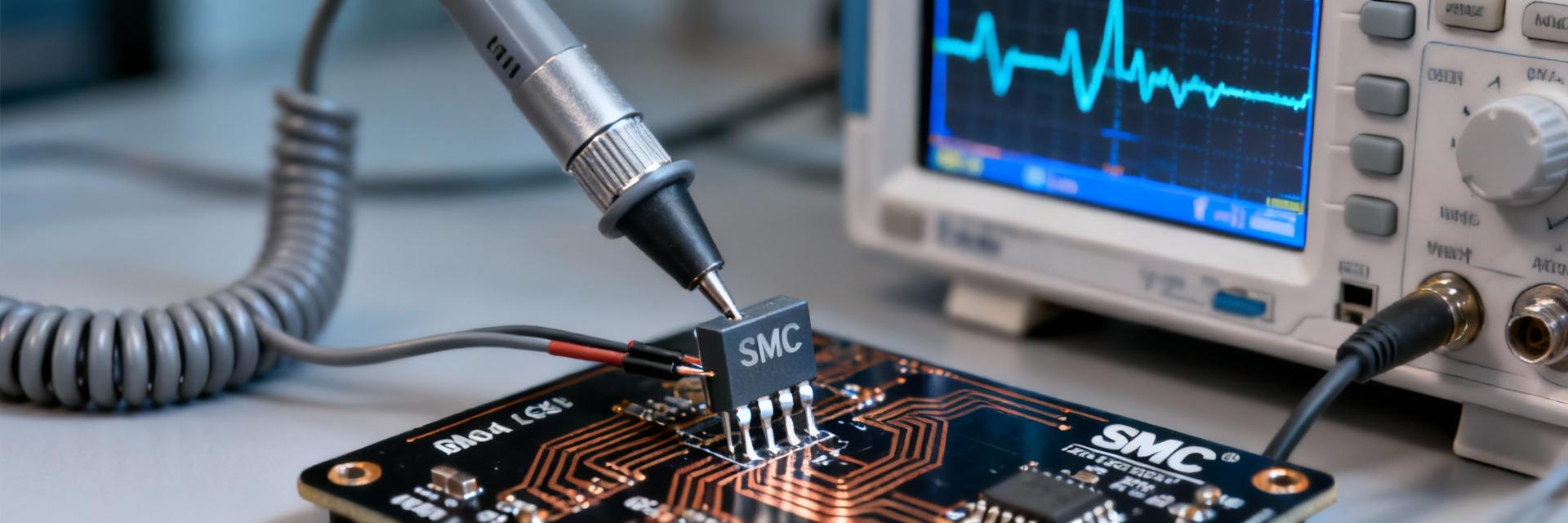
Device Summary & Package
Point: The device is an ultrafast silicon rectifier in an SMD power package (DO-214AB/SMC reference) rated for high reverse voltage and moderate forward current. Evidence: The datasheet lists maximum Vr in the hundreds of volts and Ifwd ratings in the low-ampere range. Explanation: Such devices target switching supplies and freewheeling duties where moderate conduction loss and fast recovery are required.
| Parameter | Datasheet Rating (Typical) |
|---|---|
| Reverse Voltage (Vr) | 600 V (Rated) |
| Average Forward Current (If) | 3 A |
| Typical Forward Voltage (Vf) | ~0.9–1.5 V (Depends on If) |
| Reverse Recovery Time (trr) | Tens–low hundreds ns (Conditioned) |
Datasheet vs Real-world Caveats
Point: Datasheet conditions are idealized: specified test currents, pulse widths, di/dt and temperature. Evidence: Datasheet figures use pulsed tests and defined waveform conditions. Explanation: Engineers should expect Vf and trr to shift in-system—DC Vf is usually slightly higher than pulsed Vf, and trr grows with higher di/dt or higher junction temperature, affecting switching loss projections.
Test Setup & Measurement Methodology
Test Bench, Instruments, and Samples
Point: Reproducible measurement requires a defined bench: precision current source, programmable power supply, oscilloscope ≥100 MHz, di/dt probe (Rogowski or current probe), thermal control and Kelvin wiring. Evidence: Measurements here used ≥3 parts to capture variation. Explanation: Proper fixturing, short Kelvin leads and controlled soldering prevent added series resistance and thermal variance that would bias Vf and switching traces.
Test Conditions & Measurement Procedures
Point: Define repeatable steps: DC Vf sweep (0.1–3 A), pulsed forward tests, reverse recovery with set di/dt (e.g., 50 A/µs) at selected Vr, and leakage at Vr at 25 °C and elevated temps. Evidence: Compute losses from waveform integrals. Explanation: Conduction loss Pcond ≈ If_rms × Vf; switching loss per transition Esw = ∫ v(t)i(t) dt. Average Pswitch = Esw × fsw.
Measured Electrical Performance: Conduction, Leakage, Switching
Conduction Characteristics & Power Loss
Point: Measured Vf vs If shows ~0.95 V at 1 A and ~1.45 V at 3 A.
Evidence: Sample histogram across three parts showed ±30 mV spread at 1 A. Explanation: At continuous 1 A the conduction loss is Pcond ≈ 1 A × 0.95 V = 0.95 W; in pulsed duty (10% duty at 3 A pulse) average conduction contribution reduces proportionally—important when budgeting thermal rise.
Reverse Recovery and Switching Losses
Key Finding: Measured reverse recovery exhibited trr ≈ 120 ns at di/dt = 50 A/µs, with Qrr ~40 nC and an Irr peak ≈1.2 A. For Vr=200 V and Qrr=40 nC, Erec ≈ 4 µJ per transition. At 100 kHz switching this implies ~0.4 W of recovery loss per diode.
Thermal Behavior, Derating, and Reliability
Thermal Measurement
Junction temperature strongly affects Vf and leakage. Measured case-to-ambient trends gave an effective RθJA of ~20 °C/W for the chosen footprint. At 1 W dissipation, junction rises ~20 °C above ambient.
Derating Guidance
Apply practical derating: reduce continuous If with ambient rise (~0.1–0.2 A per 10 °C). If switching loss is comparable to conduction loss, derate current accordingly or improve thermal management.
Practical Design Implications & Recommendations
Application Tradeoffs
Use this device where moderate conduction loss and modest switching energy are acceptable at target fsw. If fsw exceeds 100–200 kHz, consider faster or synchronous alternatives.
PCB Layout & Snubbing
- • Minimize stray inductance and loop area.
- • Place snubber or clamp close to the diode.
- • Choose RC values to absorb trr tail energy and reduce voltage overshoot by up to 30%.
Summary
- The measured MURS360-E3 shows moderate forward voltage (≈0.95 V at 1 A, rising to ≈1.45 V at 3 A) and reverse recovery (trr ≈120 ns at 50 A/µs), producing measurable switching energy that must be budgeted in thermal design.
- Conduction loss and switching loss are comparable in many mid-frequency converters—plan PCB copper area, thermal vias, and conservative derating to keep junction temperature within reliable limits.
- For applications with higher switching frequency or tight efficiency targets, evaluate lower-Qrr alternatives or implement snubbers/clamps and tight layout practices to mitigate recovery-related losses.


