
Overview: What the L07P020D15 current sensor is and where it fits
1.1 Key specifications at a glance
Point: The L07P020D15 is a board-mount Hall-effect open-loop current sensor specified for a nominal 20 A range with an analog voltage output and reinforced isolation. Evidence: The datasheet lists rated current, output scaling (V/A), bandwidth and isolation voltage fields. Explanation: Use the table below as a quick procurement checklist; items marked “verify” need bench confirmation (offset, bandwidth, temperature drift).
| Parameter | Datasheet value (example) | Verify on bench? |
|---|---|---|
| Nominal current rating | 20 A | No (confirm part number) |
| Topology | Hall-effect open-loop | No |
| Response time / Rise time | ≤ 1 µs | Yes |
| Bandwidth | DC – 100 kHz | Yes |
| Isolation voltage | e.g., 2000 Vrms | Yes (if safety critical) |
| Output style | Voltage proportional to current (V/A) | No |
| Package | PCB-mount | Yes (footprint fit) |
1.2 Sensor technology & operating principle
Point: The device uses an open-loop Hall-effect element positioned near a conductor; the magnetic field from conductor current produces an analog output. Evidence: Open-loop families trade lower cost and compact form factor for limited linearity and larger offset compared to closed-loop designs. Explanation: Best applications are power monitoring, motor drivers and battery management where bandwidth and isolation are required but ultra-high accuracy or very low offset are not the primary goals.
Datasheet deep-dive: interpreting electrical, mechanical & environmental specs
2.1 Electrical parameters explained (accuracy, bandwidth, response time, output scaling, isolation)
Point: Each electrical spec has practical implications: accuracy tolerances hide offset and gain error bands, bandwidth limits transient fidelity, and isolation ratings determine system creepage/clearance needs. Evidence: Datasheet accuracy often given as % of reading or % of full scale and accompanied by temperature coefficients and test conditions. Explanation: When reading the datasheet, note test conditions (ambient, RL, test frequency) and expect to verify offset at zero current, gain across the 0–20 A span, and bandwidth with a swept-frequency source; adopt tolerance bands of ±1% reading for gain and ±5 mA-equivalent for offset as initial acceptance criteria for this class.
2.2 Mechanical, thermal and compliance items
Point: Mechanical specs affect PCB cutout, mounting and safety. Evidence: Datasheet typically provides package outline, recommended PCB footprint, creepage/clearance numbers and maximum operating temperature. Explanation: Verify board cutout and standoff dimensions, confirm isolation class (basic vs reinforced), and plan mechanical fixation to avoid thermal cycling stress; if isolation is used in mains environments, insist on datasheet insulation class and re-check in procurement.
Test plan & measurement setup for L07P020D15
3.1 Test bench, instrumentation and wiring best practices
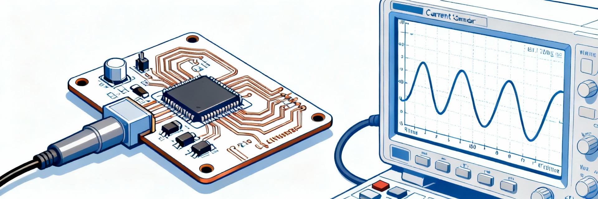
Point: Reliable measurements require a controlled bench: a low-noise programmable current source or precision source meter, an oscilloscope with ≥5× bandwidth headroom (e.g., 500 kHz scope for 100 kHz signals), and proper wiring. Evidence: Errors often originate from lead inductance, common-mode pickup and ground loops. Explanation: Use four-wire connections where possible, keep sense wiring short, use differential measurement across the sensor output with the scope or a differential amplifier, and mount the part in a PCB test jig replicating final layout to expose real coupling.
3.2 Test procedures & acceptance criteria
Point: Define repeatable procedures: zero-offset test, gain/linearity sweep 0→20 A, frequency sweep for bandwidth, step-pulse rise/fall, and temperature drift sweep. Evidence: Typical acceptance: gain within ±1% of nominal, offset within specified mV or mA-equivalent, bandwidth meeting −3 dB point near the datasheet value. Explanation: Log CSV columns: timestamp, commanded current, measured output (V), ambient temp, calculated current, error (%FS, %reading). Include plots: error vs current, Bode magnitude/phase, step response and noise histogram.
Test results: expected outcomes and how to analyze them
4.1 Accuracy, linearity and error breakdown
Point: Separate error into offset, gain, nonlinearity and temp drift. Evidence: Compute absolute error, %FS and %reading for each test point and visualize residuals and Bland–Altman style difference vs mean plots. Explanation: Residual plots will reveal slope error (gain) as a linear trend and offset as a constant bias; temperature sweeps can isolate thermal coefficients expressed in ppm/°C or mV/°C.
4.2 Bandwidth, transient response and noise performance
Point: Present bandwidth via Bode plot, step tests for rise/fall times, and RMS/peak-to-peak noise for shorted-input conditions. Evidence: A −3 dB cutoff lower than datasheet suggests downstream filtering or higher-bandwidth device. Explanation: For PWM or fast transients, ensure rise time is short enough to capture pulses; if RMS noise approaches ADC LSBs, add low-pass filtering or increase ADC sampling averaging.
Integration & application examples
5.1 PCB layout, filtering and decoupling recommendations
Point: Layout and decoupling strongly affect measured noise and offset. Evidence: Place the sensor away from high-current switching loops, route reference returns cleanly, and provide local decoupling on the sensor supply (e.g., 0.1 µF + 10 µF). Explanation: Use a single point ground for analog reference, add a small RC on the output (e.g., 1 kΩ + 100 nF) for anti-aliasing before ADC, and protect outputs with series resistors and TVS if exposed to transients.
5.2 Typical application circuits and scaling considerations
Point: The output is typically V/A; interface needs ADC scaling and potential offset compensation. Evidence: Example: if sensor outputs 50 mV/A, a 12-bit ADC with 3.3 V reference gives usable resolution—calculate conversion constants in firmware. Explanation: Implement firmware conversion: measured_V → measured_current = (measured_V - zero_offset_V) / sensitivity_V_per_A; add calibration routine to store offset and gain correction factors.
Purchasing, validation checklist & troubleshooting
6.1 Spec checklist before you buy
Point: Procurement must confirm a minimal set of datasheet fields. Evidence: At minimum verify nominal current, isolation rating and package footprint plus operating temp range. Explanation: Insist on datasheet pages for electrical characteristics, mechanical footprint PDF, and environmental ratings; obtain sample units and run the tests above prior to full production buy.
6.2 Common failure modes, diagnostics and fixes
Point: Frequent issues include offset shifts after soldering, noise coupling from switching traces, and saturation on overload. Evidence: Diagnostics: repeat zero test after reflow, inject controlled noise and observe coupling, apply overcurrent step to locate saturation point. Explanation: Mitigations include thermal reliefs on pads, improved shielding or trace rerouting, and adding series sense resistors or clamps to avoid saturation during faults.
Conclusion
Reading the L07P020D15 datasheet with a test-first mindset prevents surprises: verify offset, gain, bandwidth and isolation on a bench that mirrors the final PCB, adopt clear pass/fail tolerances, and follow layout and filtering best practices before deployment. The outlined tests and checks give a reproducible path from datasheet claims to validated system performance for any board-mount current sensor.
Key summary
- Verify offset, gain and linearity across 0–20 A; use CSV logging of commanded current, measured voltage, derived current and error for traceable analysis.
- Confirm bandwidth and rise time with frequency sweeps and pulse tests; if −3 dB is below needs, add signal conditioning or choose higher bandwidth sensor.
- Design PCB with short sense traces, single-point analog ground, local decoupling and output filtering to minimize noise and offsets for ADC interfacing.
Frequently Asked Questions
Measure the output with conductor open-circuit (zero applied current) immediately after reflow and after thermal stabilization. Record offset in volts and convert to mA-equivalent using the sensor sensitivity; if offset shifts beyond acceptance (e.g., greater than specified mV or >5 mA-equivalent), investigate solder fillets and thermal stress.
Use percent-of-reading and percent-of-full-scale metrics: for a 20 A nominal device, require gain within ±1% of reading across mid-range and nonlinearity under ±0.5% FS as a practical target for monitoring applications; tighten tolerances for precise metrology tasks.
If measured RMS noise causes ADC quantization issues or if PWM switching injects high-frequency components beyond application bandwidth, add a small RC anti-alias filter (e.g., 1 kΩ and 100 nF) and consider digital averaging; ensure the filter corner does not impede required transient response.


