-
- Contact Us
Molex 0512810894 FFC/FPC Specs: Compact Performance
The Molex 0512810894 sits at a 0.50 mm pitch and packs eight contact positions into roughly 3.5 mm of connector width, a density metric that matters for handhelds, cameras and compact industrial HMI where board real estate is constrained. This guide delivers concise, actionable data and assembly guidance for engineers evaluating or integrating the Molex 0512810894 into new designs, focusing on electrical limits, footprint and soldering best practices, reliability testing and sourcing considerations to speed prototyping and reduce rework risk.
Quick product snapshot & background (Background introduction)
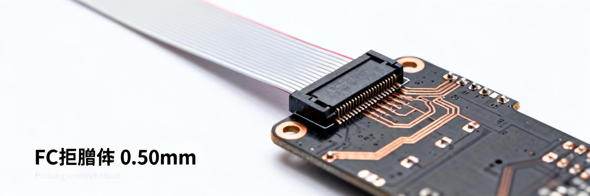
Key identification (part number, series, basic form-factor)
Point: The part is identified as 0512810894 from Molex's 51281 series — an Easy‑On™ right‑angle, surface‑mount FFC/FPC connector with 8 contacts in a non‑ZIF dual‑contact style. Evidence: the form‑factor is a right‑angle SMT body designed to accept a flat flexible cable or flexible printed cable without a top‑acting latching ZIF mechanism. Explanation: that non‑ZIF, dual‑contact configuration provides a secure press fit between cable conductor and mating contact, offering reliable signal continuity for limited‑mate/unmate use; designers should consult the official product datasheet for exact mechanical drawings and recommended land patterns when finalizing the layout.
Physical footprint at a glance
Point: Key physical numbers designers need are pitch 0.50 mm (0.020"), eight contacts spanning approximately 3.5 mm, right‑angle orientation and SMD termination pads. Evidence: the contact span is calculated as (contacts − 1) × pitch = (8 − 1) × 0.50 mm ≈ 3.5 mm; the right‑angle body shifts cable exit parallel to the PCB plane. Explanation: these figures allow rapid compatibility checks against board edge clearances and enclosure openings; early selection decisions should confirm stack height, FFC retention direction and mating orientation to avoid late redesigns.
Typical applications
Point: Typical uses include compact consumer and industrial devices where thin profiles and tight lateral space dominate. Evidence: examples—handheld instruments (compact boards, battery constraints), still/video cameras (short ribbon runs and small lens/mechanism envelopes), wearables (low profile, constrained thickness), and compact industrial HMI (space-constrained PCB regions near displays). Explanation: in each case the 0.50 mm pitch and right‑angle exit reduce PCB footprint while allowing short, secure flexible cable runs; choose the part when mating cycles are modest and cable routing is constrained.
Electrical, mechanical & environmental specifications (Data analysis)
Electrical ratings and signal performance
Point: The connector is suitable primarily for signal and light power paths, with typical ratings on the order of 50 V and ~0.5 A per contact. Evidence: typical contact resistance and insulation values for this class of FFC/FPC connector permit digital signalling and limited DC bias or LED/backlight power. Explanation: use 0.5 A per contact for short runs and distributed currents; if a single contact must carry >0.5 A continuously, redesign to increase conductor count or use a dedicated power connector to avoid thermal rise, contact heating and accelerated wear.
Mechanical specs and materials
Point: Contacts are gold plated for reliable low‑resistance mating; housing is a high‑temperature thermoplastic suitable for reflow; mating cycles are moderate. Evidence: dual‑contact designs increase contact redundancy and improve retention; recommended FFC/FPC thicknesses usually fall inside a narrow range (check datasheet for exact values). Explanation: gold plating reduces fretting corrosion for signal integrity, while the thermoplastic housing tolerates standard lead‑free reflow profiles; designers should verify the specified number of mate/unmate cycles to ensure lifecycle alignment with product requirements.
Environmental limits and compliance
Point: Operating temperature ranges and RoHS compliance are typical considerations; cleaning/flux compatibility matters. Evidence: the connector class commonly supports commercial to extended temperature ranges and is offered in RoHS‑compliant finishes. Explanation: validate the component's specified temperature range against your device's thermal environment and select appropriate cleaning methods (e.g., no aggressive solvents against the housing) to avoid embrittlement or residue that could affect contacts.
PCB footprint, layout & soldering best practices (Method / how-to)
Recommended PCB land pattern and solder paste stencil guidelines
Point: Proper pad sizing and controlled paste apertures reduce tombstoning and ensure reliable solder fillets under right‑angle SMT bodies. Evidence: for 0.50 mm pitch SMD connectors, paste coverage typically targets 60–80% of pad area with slightly reduced center apertures to avoid excess solder. Explanation: use manufacturer‑recommended land patterns as a starting point; tune paste aperture (e.g., 0.6–0.7 of pad) to balance wetting and prevent bridging. Where possible, add small copper thieving pads or solder thieving to equalize solder volumes across the row.
Placement, reflow profile & assembly tips
Point: Orientation during reflow, nozzle selection for pick‑and‑place and a lead‑free reflow window are key for consistent yields. Evidence: right‑angle SMD connectors benefit from placing the body toward the board centre so gravity and solder wetting stabilize part during reflow. Explanation: program placement machines with a nozzle sized to the connector footprint and use the recommended peak temperature and soak times from the component datasheet; consider bottom‑side support or tack reflow steps for long rows to prevent movement.
Design-for-test and repairability
Point: Testability and rework access reduce field failures and speed debugging. Evidence: include test vias or accessible test points on the cable's signal traces and leave clearance for hot‑air or localized IR rework. Explanation: plan inspection access (optical, and X‑ray where needed), position test points away from the connector edge for probe access, and document a rework procedure specifying hot‑air temperature and nozzle size to avoid melting the right‑angle housing.
Reliability, testing & failure modes (Data + method)
Common failure modes and mitigation
Point: Failures usually arise from misalignment, poor solder joints, flex cycle wear or contact contamination. Evidence: intermittent opens from cold solder joints or signal degradation from worn contacts are typical failure signatures. Explanation: mitigate by using fiducials and accurate assembly vision for alignment, proper paste control to avoid cold joints, strain relief for the FFC/FPC to reduce flex at the termination, and specifying gold plating/cleaning regimes to resist contamination.
Test protocols to validate assembly
Point: Combine electrical, mechanical and environmental tests to validate connector performance in application. Evidence: recommended checks include continuity and contact resistance measurements, mate/unmate cycling to the specified cycle count, thermal cycling and humidity stress. Explanation: include pass/fail thresholds tied to contact resistance delta and leakage limits; design sample test matrices that exercise both static solder integrity and dynamic flex of the cable to capture early wear modes.
Failure analysis tips and instrumentation
Point: Microscopy, X‑ray and targeted electrical logging are effective to reproduce and diagnose intermittent faults. Evidence: cross‑section analysis and X‑ray reveal voided solder joints; time‑domain logging can capture intermittent opens during flex. Explanation: when facing an intermittent, instrument the cable and board to log contact resistance under expected mechanical motion, use high‑magnification inspection to find fretting or contamination, and use X‑ray to confirm solder voids or misalignment beneath pads.
Alternatives, sourcing & cost considerations (Case / comparative)
Direct equivalent parts and form-fit replacements
Point: When seeking equivalents, match pitch, orientation, contact count and mechanical footprint first. Evidence: a direct form‑fit replacement must match the 0.50 mm pitch, 8 positions, right‑angle termination and pad geometry to avoid PCB changes. Explanation: verify datasheets side‑by‑side for critical dimensions and electrical ratings; if the footprint differs slightly, calculate PCB redesign effort and consider adapters only when cost and schedule justify the change.
Performance vs. cost trade-offs
Point: Choose between non‑ZIF vs ZIF designs, and gold plating grades versus commodity finishes based on expected mating cycles and signal integrity needs. Evidence: ZIF mechanisms ease assembly and reduce cable abrasion but add cost and height; single‑contact designs are cheaper but may offer less reliability than dual‑contact in high‑vibration environments. Explanation: invest in higher‑grade plating and dual‑contact designs when long lifecycle or harsh environments are expected; choose commodity options for disposable or low‑cycle consumer applications.
Distributor availability, lead times & purchasing tips
Point: Check multiple authorized distributors and validate reel/tray packing and part numbering (51281 vs 0512810894 naming variants). Evidence: lead times can vary by vendor; minimum order quantities and reel packaging affect prototype vs production procurement. Explanation: use approved vendors, request certificate of conformity, and consider small trial reels for prototyping; perform counterfeit checks and confirm the exact manufacturer part numbering before placing production orders.
Design checklist & actionable next steps for engineers (Action recommendations)
Pre-design checklist (quick pass/fail)
Point: A short pass/fail list avoids late surprises. Evidence: confirm pitch, contact count, current/voltage, FFC thickness, mating cycles, PCB footprint and DFM constraints before layout. Explanation: include verification items such as physical cable thickness, required retention force, maximum ambient temperature and whether shielding/grounding is needed; if any item fails, select an alternate connector early to avoid a board respin.
Prototyping and verification plan
Point: Define sample quantities and a staged test plan for early validation. Evidence: order a small quantity of parts on reel, build 3–5 prototype units, and run electrical continuity, flex‑cycle and thermal tests. Explanation: schedule one revision after initial assembly based on test feedback; ensure test fixtures and probe points are available so lab validation can be repeated across firmware/hardware iterations.
Procurement & long-term lifecycle considerations
Point: Stock and lifecycle planning reduce field risk. Evidence: maintain safety stock sized to lead times and monitor manufacturer change notifications; prefer footprints that accept multiple vendors. Explanation: avoid single‑source risks by selecting common footprint families and tracking approved equivalents to simplify last‑minute sourcing changes as demand scales.
| Spec | Typical Value |
|---|---|
| Pitch | 0.50 mm (0.020") |
| Contacts | 8 positions (span ≈ 3.5 mm) |
| Orientation | Right‑angle, SMT |
| Typical Voltage | 50 V |
| Typical Current per contact | ~0.5 A |
| Contact finish | Gold plating |
Summary
The Molex 0512810894 is a compact, 8‑position FFC/FPC connector at 0.50 mm pitch designed for tight lateral real estate and right‑angle cable exits. Top cautions are validating the PCB footprint and paste stencil, confirming soldering and reflow procedures, and performing flex‑cycle validation under intended environmental conditions. Actionable recommendation: prototype with production‑grade cables and run a focused test matrix (continuity, mate/unmate cycles, thermal/humidity stress) before committing to a production PCB revision.
- Compact form factor: 8 positions at 0.50 mm pitch (span ≈ 3.5 mm), suitable for space‑constrained designs and FFC/FPC connector applications.
- Electrical limits: ~50 V rating and ~0.5 A per contact—ok for signals and light power; redesign if higher continuous current is required.
- Assembly controls: use recommended land pattern, controlled paste coverage and right‑angle placement best practices to avoid tombstoning and cold joints.
- Reliability focus: validate flex cycles, strain relief and contact resistance over environmental stress tests to catch wear and intermittent faults early.
- Sourcing: confirm vendor part numbering and packaging, keep safety stock and prefer footprints compatible with multiple vendors.
FAQ
What are the electrical ratings for Molex 0512810894 and is it suitable for power?
Answer: The connector is intended primarily for signal use with a nominal 50 V rating and roughly 0.5 A per contact in typical applications. It can support small power loads distributed across multiple contacts, but for sustained high current on a single conductor designers should opt for dedicated power connectors or increase conductor count to reduce heating and contact stress.
How should engineers handle PCB footprint and solder paste for Molex 0512810894?
Answer: Engineers should start with the manufacturer's recommended land pattern and tune solder paste apertures to 60–80% coverage to minimize bridging and tombstoning. Use a stencil with slightly reduced center apertures for the inner pads and ensure reflow profile matches the housing and finish; validate with a prototype board and visual/X‑ray inspection.
What reliability tests should be run on assemblies using Molex 0512810894?
Answer: A practical validation plan includes continuity and contact resistance checks, mate/unmate cycling to the specified cycle count, thermal cycling and humidity/soak tests, and mechanical flex cycling of the FFC/FPC with logged electrical monitoring to detect intermittent faults; perform microscopy and X‑ray as part of failure analysis if anomalies appear.
- Technical Features of PMIC DC-DC Switching Regulator TPS54202DDCR
- STM32F030K6T6: A High-Performance Core Component for Embedded Systems
- Tamura L34S1T2D15 Datasheet Breakdown: Key Specs & Limits
- PAL6055.700HLT Datasheet: Complete Technical Report
- FDP027N08B MOSFET Datasheet Deep-Dive: Key Specs & Test Data
- LT1074IT7: Complete Specs & Key Parameters Breakdown
- How to Verify G88MP061028 Datasheet and Specs - Checklist
- NFAQ0860L36T Datasheet: Measured IPM Performance Report
- 90T03P MOSFET: Complete Specs, Pinout & Ratings Digest
- 3386F-1-101LF Datasheet & Specs — Pinout, Ratings, Sources
-
 MM74HC4050NSanyo Semiconductor/onsemiIC BUFFER NON-INVERT 6V 16DIP
 -
 MM74HC4049NSanyo Semiconductor/onsemiIC BUFFER NON-INVERT 6V 16DIP
 -
 MM74HC4040NSanyo Semiconductor/onsemiIC BINARY COUNTER 12-BIT 16DIP
 -
 MM74HC4020NSanyo Semiconductor/onsemiIC BINARY COUNTER 14-BIT 16DIP
 -
 MM74HC393NSanyo Semiconductor/onsemiIC BINARY COUNTR DL 4BIT 14MDIP
 -
 MM74HC374NSanyo Semiconductor/onsemiIC FF D-TYPE SNGL 8BIT 20DIP
 -
 MM74HC373NSanyo Semiconductor/onsemiIC D-TYPE TRANSP SGL 8:8 20DIP
 -
 LT1213CS8Linear Technology (Analog Devices, Inc.)IC OPAMP GP 2 CIRCUIT 8SO
 -
 MM74HC259NSanyo Semiconductor/onsemiIC LATCH ADDRESS 8BIT 16-DIP
 -
 MM74HC251NSanyo Semiconductor/onsemiIC MULTIPLEXER 1 X 8:1 16DIP

