-
- Contact Us

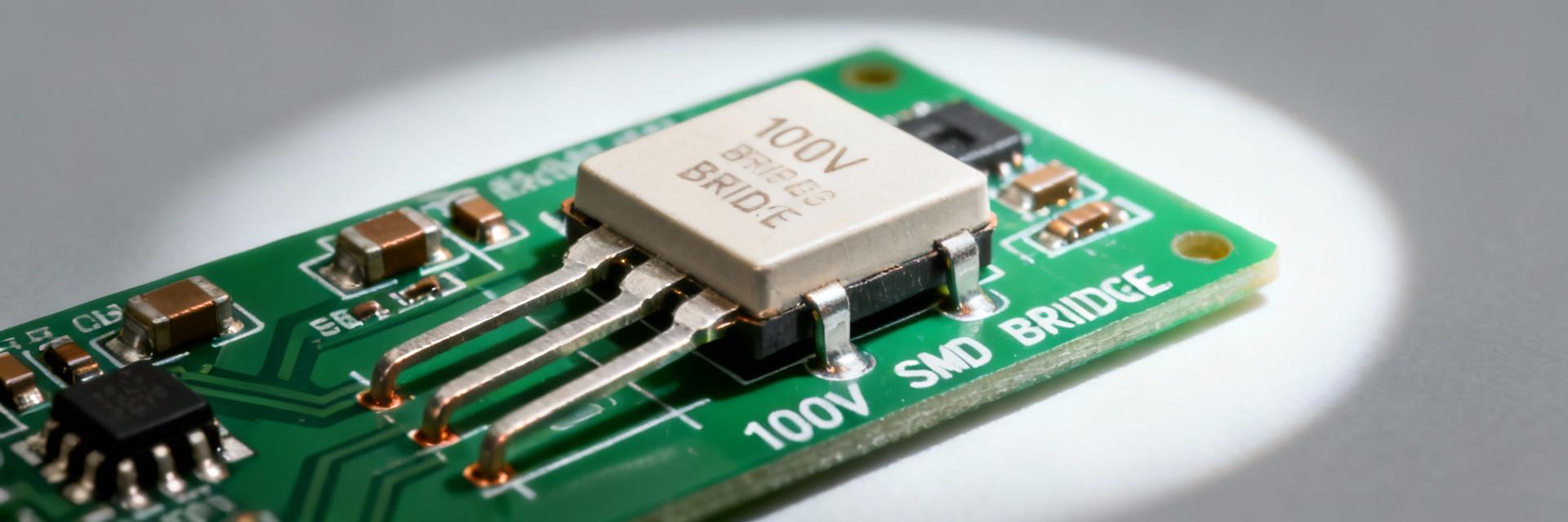
ABS10A-13 Datasheet Deep Dive: Specs & Insights for Engineers
The ABS10A-13 is a 1.0 A surface-mount glass-passivated bridge rectifier rated for high blocking voltage—peak repetitive reverse voltage up to 1000 V—and characterized by a maximum forward voltage around 1.1 V at 1 A and reverse leakage down to single-digit microamperes at full PRV. These headline numbers are the practical starting point every design engineer needs when reading the ABS10A-13 datasheet and translating lab figures into board-level decisions. This article walks engineers through the critical datasheet entries, shows how to apply the specs in real designs (loss, thermal, surge), and gives practical test, sourcing, and substitution guidance you can act on in pre-production.
1 — ABS10A-13 at a glance (Background)
Key datasheet numbers and what they mean
Point: The must-capture metrics from the ABS10A-13 datasheet are Io (1.0 A), maximum forward voltage Vf (≈1.1 V @ 1 A), peak repetitive reverse voltage (PRV) up to 1000 V, reverse leakage (µA scale at high VR), non-repetitive surge current IFSM, and operating junction temperature limits. Evidence: The manufacturer’s datasheet lists these ratings as the device’s electrical and thermal boundaries. Explanation: For design use, Io sets continuous RMS conduction capability, Vf governs conduction loss (Pcond ≈ Vf × I), PRV defines blocking safety for mains-derived isolation, and leakage and IFSM determine suitability for high-voltage low-current sensing versus surge-prone mains front ends. Capture these numbers in your component spec sheet before layout or procurement.
Package, footprint and mechanical details
Point: ABS10A-13 is supplied in a compact SMD bridge package common to low-power rectifiers (check SOPA-4 / SMD outline in the datasheet). Evidence: Package drawings in the mechanical section identify pad pitch, overall dimensions, and polarity markings. Explanation: On the PCB, verify pad land dimensions against the manufacturer mechanical drawing, mark polarity clearly (corner pad or molded triangle), and adjust pad-to-pad spacing for high-voltage creepage if using the 1000 V rating. For reliable reflow, follow the solder paste stencil recommendations and note any thermal pad or courtyard callouts on your fab drawing.
Typical applications and selection rationale
Point: Typical uses include AC→DC bridge for small SMPS, high-voltage LED drivers, chargers, and mains sensing circuits where voltage headroom is primary and currents are modest. Evidence: The device’s 1 A continuous rating with high PRV makes it a natural fit for low-power, high-voltage lines. Explanation: Choose ABS10A-13 when you need high blocking voltage with compact SMD packaging; avoid it if continuous currents approach the multi-amp range or if Vf-related power loss cannot be tolerated. For example, a low-current LED driver that needs 700–900 V blocking with
| Parameter | Typical / Max |
|---|---|
| Continuous forward current (Io) | 1.0 A |
| Max forward voltage (Vf) | ≈1.1 V @ 1 A |
| Peak Repetitive Reverse Voltage (PRV) | Up to 1000 V |
| Reverse leakage | ~5 µA @ 1000 V (typical order) |
| Package | SOPA-4 / SMD bridge |
2 — Electrical characteristics deep-dive (Data analysis)
Forward behavior: Vf, dynamic resistance, and power dissipation
Point: Forward conduction loss is the product of Vf and forward current; dynamic resistance and temperature dependence modify Vf across operating ranges. Evidence: Datasheet Vf vs If curves and typical dynamic resistance entries quantify how Vf climbs with current and temperature. Explanation: Use Pcond = Vf × I to estimate steady-state loss. Worked example: at 0.5 A, if Vf is 0.9–1.0 V (interpolated from the Vf curve), Pcond ≈ 0.5 A × 1.0 V = 0.5 W. Account for temperature—Vf typically increases with junction temperature for silicon rectifiers, so thermal rise can increase loss slightly and feed back into junction temperature. Include dynamic resistance in transient models for accurate drop predictions in pulse conditions.
Reverse specs: PRV, VRRM, leakage and avalanche considerations
Point: Peak Repetitive Reverse Voltage (PRV) defines the maximum continuous reverse stress the part can see; datasheet curves clarify non-repetitive limits and avalanche behavior. Evidence: The datasheet differentiates PRV ratings and provides leakage vs. VR and temperature plots. Explanation: For high-voltage, low-current circuits, leakage matters more than conduction loss; a few microamperes of leakage at 1000 V can bias sensitive measurement nodes. Use a safety margin—typically 20–30% above expected peak reverse stress—when selecting VR to accommodate voltage spikes and manufacturing tolerance. Avoid operating at the absolute PRV limit without adequate transient suppression.
Transient & surge performance (IFSM, non-repetitive surge)
Point: IFSM (peak non-repetitive forward surge current) describes the device’s ability to survive short high-current pulses, often specified for a half-sinewave of 8.3 ms for mains surge testing. Evidence: Datasheet surge curves and IFSM ratings indicate allowable short-duration currents and thermal limits. Explanation: Read the IFSM curve to determine whether expected inrush or fault currents (e.g., capacitor charging or transformer magnetizing inrush) exceed the device’s capability. If near or above, add soft-start, inrush limiting, or a snubber; for repeated surges, choose a part with higher IFSM or derate Io to reduce stress. Always calculate energy (I^2·t) for the expected waveform and compare to datasheet non-repetitive-energy curves.
3 — Thermal, derating & reliability (Data analysis / Method)
Thermal resistance, junction temp, and derating curves
Point: Junction temperature Tj = Ta + P × RθJA (or use RθJC plus heatsink path) is the primary thermal relation; derating curves show allowable Io vs ambient. Evidence: Datasheet provides RθJA / RθJC and derating guidance; combine with measured or estimated dissipation to compute Tj. Explanation: Example method—if Pcond = 0.5 W and RθJA = 60 °C/W (confirm exact datasheet value), ΔTj ≈ 30 °C; at Ta = 60 °C, Tj ≈ 90 °C which is within typical silicon limits. Use datasheet derating curves to reduce continuous Io at elevated ambient: many SMD bridge rectifiers require derating above a baseline temperature (check the curve) to preserve long-term reliability.
PCB mounting, thermal vias and practical cooling tips
Point: Board-level thermal management—copper pours, thermal vias, solder volume—significantly affects RθJA and thus junction temperature. Evidence: Manufacturer layout recommendations and general SMD thermal practice show pad sizes and via patterns to reduce thermal resistance. Explanation: To lower junction temperature, maximize copper area connected to the device’s pads, add thermal vias under large pads to inner or back-side copper planes, and avoid isolated small pads. For reflow, respect profile recommendations to ensure full wetting; inconsistent soldering raises contact resistance and worsens thermal paths. Include thermal validation steps (IR thermography, in-situ Tj measurement) in your sign-off plan.
Reliability, operating limits and failure modes
Point: Typical operating junction ranges are broad (for many silicon devices from about −55 °C to +150 °C storage and similar operating limits); common failures include thermal overstress and surge-induced junction degradation. Evidence: Datasheet specifies operating and storage temperature ranges and notes on non-repetitive stress. Explanation: Mitigate failure modes by ensuring Tj stays well below max during worst-case ambient and power dissipation, by limiting repetitive surge exposure, and by applying appropriate burn-in or thermal-cycle tests during qualification. For long-life designs, target average operating temperatures well below maximum to improve MTBF.
4 — Test procedures & bench validation (Method / Action)
How to measure Vf, reverse leakage, and PIV safely
Point: Use controlled current sources and high-voltage sources with limited energy for PIV testing; measure Vf with a precision supply and series sense resistor, and measure leakage with a picoammeter at rated VR. Evidence: Standard bench practice and datasheet test conditions call out currents, pulse durations, and measurement temperatures. Explanation: For Vf measure at 1 A, use a source capable of delivering the current and measure the drop across the diode with a four-wire sense if possible. For reverse leakage and PIV, ramp voltage slowly while monitoring current; use HV supplies with current limiting to avoid destructive avalanching. Note pass/fail thresholds from the datasheet and log temperature during measurement, as leakage scales with Tj.
Surge, ESD and thermal cycling test protocols
Point: Define test sequences that replicate expected field stress—single short surge (IFSM-style), ESD contact/discharge checks, and thermal cycling to rated extremes. Evidence: Datasheet surge specs and industry test standards guide waveform selection and cycle counts. Explanation: Execute controlled surge tests (e.g., half-sine 8.3 ms) while monitoring device Vf and leakage before/after; use ESD testers for IEC-style levels relevant to your product. For thermal cycling, use the junction/storage ranges from the datasheet and inspect for drift versus catastrophic failure. Record results in a test report with pre/post electrical characteristics for traceability.
Troubleshooting discrepancies between datasheet and measured behavior
Point: Discrepancies often stem from measurement setup, soldering damage, lot variation, or temperature misestimation. Evidence: Common root causes are documented in field reports and supplier application notes. Explanation: Isolate issues by cross-checking fixtures (four-wire, recommended sweep rates), swapping to a fresh sample from a different reel, and inspecting solder joints and package markings. If behavior persists, gather full test logs, photos, lot/date codes, and waveform captures before contacting supplier support—this speeds root-cause analysis and warranty/quality handling.
5 — Sourcing, alternatives and design checklist (Case study / Action)
Comparing ABS10A-13 to similar bridge rectifiers
Point: When substituting, match PRV, Io, Vf, package, and thermal resistance; differences in RθJA or leadframe can break thermal equivalence. Evidence: Side-by-side spec comparisons show identical VR and Io do not guarantee equal thermal performance. Explanation: Create a short spec-comparison table for candidate parts and prioritize matching PRV and Io first, then Vf and package. If RθJA differs, run thermal simulations or margin the Io downward. For drop-in replacement, ensure mechanical pad compatibility and reflow profile compatibility.
| MPN | PRV (V) | Io (A) | Vf @1A (V) | Package |
|---|---|---|---|---|
| ABS10A-13 | 1000 | 1.0 | 1.1 | SMD bridge |
| Competitor X | 600 | 1.0 | 1.0 | SMD bridge |
Procurement, packaging, and counterfeit checks
Point: Order from authorized distributors, track reel/lot codes, and inspect incoming parts for visual anomalies. Evidence: Distributor traceability and manufacturer packaging notes reduce counterfeit risk. Explanation: Typical packaging is tape-and-reel for SMD bridges; verify part markings, packaging seals, and date codes. Red flags include inconsistent marking, unusual finish, or price significantly below market. Implement basic incoming tests (Vf spot check, leakage at VR) for suspect lots before assembly to avoid rework.
Pre-production design checklist & recommended BOM notes
Point: Consolidate footprint checks, thermal simulation, bench verification, derating confirmation, and supplier qualification into a pre-PN checklist. Evidence: Design for manufacturability and quality control best practices recommend these steps. Explanation: Suggested BOM line: exact MPN, manufacturer name, package, and approved alternates with distinct part numbers. Checklist items: verify mechanical drawing vs footprint, run thermal sims at worst-case power, bench test samples for Vf/leakage/IFSM, confirm derating at expected ambient, and qualify supplier traceability.
Summary
- The ABS10A-13 provides 1.0 A continuous current and high blocking capability (1000 V PRV), making it suitable for low-current, high-voltage AC→DC bridge roles where compact SMD form factor matters; confirm Vf and leakage tradeoffs before commit.
- Use Vf × I for conduction loss estimates, combine with RθJA to predict junction temperature, and apply a 20–30% VR margin for transient headroom; always check the manufacturer datasheet for precise Rθ and surge curves.
- Validate with bench tests (Vf at 1 A, leakage at rated VR, IFSM surge tests), implement PCB thermal best practices (copper pours, vias), and enforce procurement checks for traceability and counterfeit avoidance.
FAQ
What are the key specs in the ABS10A-13 datasheet I should record?
Record Io (1.0 A), Vf at relevant test current (≈1.1 V @ 1 A), PRV/VR rating (1000 V), reverse leakage at VR and temperature, IFSM surge rating and the specified waveform, package outline, and RθJA/RθJC. These fields let you simulate loss, thermal rise, surge tolerance, and PCB layout implications.
How do I calculate junction temperature for ABS10A-13 in my board layout?
Compute Tj = Ta + P × RθJA where P ≈ Vf × I + switching or ripple losses. Use the datasheet RθJA for the recommended mounting; if you added copper pours or vias, measure RθJA in a thermal test coupon. Validate with IR or junction-sensing techniques during prototype to ensure design margins.
Can I drop in a different bridge for ABS10A-13 without revalidation?
Only if the substitute matches PRV, Io, Vf, package footprint, and thermal resistance. Even then, differences in RθJA or mechanical leadframe can change thermal performance—revalidation (thermal and surge tests) is strongly recommended before production to avoid field failures.
-
 BLM18AG102SN1D Murata: Latest Datasheet & Key Specs2025-12-22 12:49:40 0BLM18AG102SN1D provides 1,000 Ω impedance ±25% at 100 MHz, 450 mA rated current and 0.5 Ω max DC resistance — making it a common 0603 ferrite bead choice for EMI suppression in compact designs. This part matters to PCB designers because it balances high-frequency attenuation with modest series loss, useful for power-rail noise control in consumer and industrial electronics. The following synthesizes the latest datasheet highlights, practical layout and thermal guidance, verification steps and substitution rules so engineers can decide quickly whether the Murata bead fits their design constraints. #1 — Quick background: What is BLM18AG102SN1D and where it fits Core identity & key use cases Point: BLM18AG102SN1D is a Murata BLM-series SMD ferrite bead in an 0603 (1608 metric) package used for targeted EMI suppression. Evidence: Datasheet nominal values show 1 kΩ impedance at 100 MHz and a 450 mA rated current. Explanation: That combination makes this bead ideal for single-line power filtering near ICs, choke function on sensitive signal traces, and decoupling chains where PCB real estate is limited. Refer to the Murata datasheet for official mechanical and electrical dimensions. How this part compares inside Murata’s BLM family Point: Within the BLM family, variants trade impedance, DC resistance and current handling. Evidence: Compared to lower-impedance 0603 beads, the 1 kΩ class raises high-frequency attenuation but increases series loss and thermal stress at high DC. Explanation: Choose this 1 kΩ@100 MHz bead when conducted noise sits in the 10–500 MHz band and available margin for series resistance is acceptable; choose lower-impedance BLMs for higher-current rails or where voltage drop must be minimized. #2 — Datasheet highlights: Absolute electrical specs & performance Electrical ratings (must include exact figures) Point: Key absolute values determine allowable in-system use. Evidence: Impedance = 1,000 Ω ±25% @ 100 MHz; rated current = 450 mA (at upper operating conditions); DC resistance (max) = 0.5 Ω; single circuit. Explanation: These figures imply designers should derate working current for sustained thermal loading and verify insertion loss on populated boards rather than rely solely on free-air datasheet numbers. ParameterValue Impedance (100 MHz)1,000 Ω ±25% Rated current450 mA DC resistance (max)0.5 Ω Package0603 (1608 metric) Frequency response and EMI suppression behavior Point: Ferrite beads show frequency-dependent impedance rather than a simple inductive response. Evidence: The datasheet impedance-vs-frequency curve peaks in the 10s–100s of MHz, delivering resistive damping where EMI energy concentrates. Explanation: For designers this means the BLM18AG102SN1D attenuates high-frequency noise effectively; however, impedance drops outside its optimal band and it should not be used where broadband low-frequency filtering is required. #3 — Thermal, reliability & assembly guidance (practical design rules) Thermal limits and rated current practice Point: Operating temperature and current interact to change bead behavior. Evidence: Typical operating ranges span low-to-high ambient conditions and rated current is specified for acceptable deformation of characteristics. Explanation: Engineers should margin the 450 mA rating by accounting for PCB copper heat-sinking, ambient temperature, and duty cycle. Use temperature-rise measurements on a populated board to validate steady-state loss and avoid long-term impedance drift. Soldering, footprint, and packaging notes Point: Correct land pattern and reflow profile preserve performance and assembly yield. Evidence: Murata mechanical drawings list land pads for 0603 beads and recommend standard SnAgCu reflow thermal profiles. Explanation: Use manufacturer-recommended footprint to avoid tombstoning or lift; order in reel quantities for pick-and-place; treat as passive parts with typical handling and ESD precautions. Check the datasheet for exact pad dimensions before final PCB CAM. #4 — Design examples & real-world application patterns Typical circuit placements and layout best practices Point: Placement determines effectiveness. Evidence: Practical layouts put the bead either at source (to block upstream noise) or at load (to protect sensitive ICs), often paired with a decoupling capacitor to form an RC notch. Explanation: Keep traces short on both sides, minimize parallel loops, place bead close to the pin being protected, and avoid adding series inductance that could form unwanted resonances with local capacitance. Real-world use cases and measured results Point: Measured attenuation and S-parameter tests validate choices. Evidence: Bench tests commonly show several dB to tens of dB reduction in conducted noise within the bead’s effective band. Explanation: Measure insertion loss and S21 on the populated board; use time-domain probing to verify ripple reduction on power rails. Remember the bead also adds small series resistance that can affect low-voltage rails under heavy load. #5 — Sourcing, equivalents, and verification checklist (actionable next steps) Where to get the official datasheet and how to verify part authenticity Point: Always download the official PDF before release. Evidence: The manufacturer’s product information module and authorized distributors carry the latest revision. Explanation: Verify package code, ordering suffixes (e.g., reel or cut-tape variants), RoHS/REACH declarations and reel size. Cross-check markings and batch codes on samples against the manufacturer specification to ensure authenticity. Cross-references and equivalent parts Point: Substitutes require matching multiple parameters. Evidence: Equivalents must be compared on impedance at 100 MHz, rated current, DCR and package. Explanation: When swapping parts search for “ferrite bead 0603 1kΩ 450mA” and perform A/B tests on a pilot run to confirm thermal and EMI performance before wide substitution. Summary BLM18AG102SN1D is a compact 0603 Murata ferrite bead delivering ~1 kΩ impedance at 100 MHz with a 450 mA rating and 0.5 Ω max DCR, suitable for targeted EMI suppression near ICs and on power rails. Designers should validate current derating and temperature rise on the populated PCB, pair the bead with nearby decoupling capacitors, and follow Murata land-pattern recommendations from the datasheet. Before substituting alternatives, match impedance curve shape, DCR and thermal behavior, and run insertion-loss measurements on a prototype to verify real-world suppression. Frequently Asked Questions How should I validate BLM18AG102SN1D performance on my PCB? Measure insertion loss (S21) on the populated board across the target frequency band and perform time-domain probing of the supply rail under representative loads. Compare measured impedance and temperature rise against expected datasheet behavior and adjust placement or add decoupling as needed. What footprint and reflow considerations apply to this ferrite bead? Use the Murata-recommended 0603 land pattern to minimize solder-attach issues; follow standard SnAgCu reflow profiles and control ramp rates to prevent tombstoning or excessive thermal stress. Handle reels with normal passive-component precautions and verify pad solderability on the PCB stack-up. Which parameters are most critical when selecting an equivalent part? Prioritize matching impedance at 100 MHz, rated DC current and maximum DC resistance, then verify the impedance-vs-frequency curve shape and thermal derating. Always pilot-test substitutes on a small production run to confirm EMI and power-integrity outcomes.READ MORE
 -
 TCD2709DG How-to: Optimize Readout & Reduce Smear in CCD2025-12-21 12:47:36 0Point: Engineers integrating the TCD2709DG face two persistent issues: suboptimal readout (speed, noise, dynamic range) and visible smear in images. Evidence: Bench reports and integration logs commonly show elevated trailing near bright targets and slower effective line rate after conservative timing. Explanation: This guide delivers a compact, testable workflow covering measurement, clocking, PCB hygiene, optical mitigation, and post-processing to reduce smear and optimize readout. Point: The approach prioritizes measurable steps and repeatable tests. Evidence: Each section maps to simple captures, oscilloscope checks, and before/after logging for objective comparison. Explanation: Use the provided checklist to document baseline metrics, apply incremental fixes, and iterate until readout performance and image cleanliness meet system requirements. 1 — Background: What the TCD2709DG Is and Why Readout & Smear Matter 1.1 Overview of the TCD2709DG Point: The TCD2709DG is a line-scan CCD used in machine-vision and spectroscopy contexts. Evidence: System integrators consult the official datasheet for absolute timing, voltage limits, and recommended clock sequences rather than relying on assumed specs. Explanation: For safe optimization, always cross-check any timing or amplitude changes against the datasheet to avoid damage and to respect specified transfer windows. 1.2 What Is Smear and How It Appears in CCDs Point: Smear is charge accumulated or shifted during transfer that produces bright-source trails along the transfer axis. Evidence: In practice, smear manifests as linear streaks from saturated regions during vertical or line transfers, distinct from bloom which is charge spilling between pixels. Explanation: Look for asymmetric trails aligned with read direction and for intensity that scales with bright-source exposure time to distinguish smear from other artifacts. 2 — Data Analysis: Measuring Your Readout Performance & Smear Metrics 2.1 Readout performance metrics to measure Point: Key measurable metrics are readout speed (lines/s), read noise (e− rms), linearity, dynamic range, and ADC quantization error. Evidence: Typical test sets include dark frames for noise, flat fields for linearity and PRNU, and timing captures for line-rate validation. Explanation: Combine sensor captures with oscilloscope traces of clock rails and ADC sample windows to correlate electrical behavior with pixel-level outcomes. 2.2 Quantifying smear: practical tests and expected outcomes Point: Quantify smear with controlled tests such as single bright-line exposures, slanted-edge highlights, and timed transfer sequences. Evidence: Compute smear percentage as the integrated trailing signal divided by the source signal, and plot vertical profiles to isolate transfer-direction decay. Explanation: Log baseline smear values per scene and application tolerance (spectroscopy vs. machine inspection have different acceptability) for A/B comparison after each mitigation step. 3 — Readout Optimization: Hardware & Timing Adjustments 3.1 CCD clocking, timing, and driver best practices Point: Optimal clock amplitudes and edge shaping reduce spurious charge and improve charge transfer efficiency (CTE). Evidence: Oscilloscope checks often reveal ringing or slow edges that correlate with increased CTI and smear. Explanation: Use controlled slew rates, short matched traces to drivers, and implement pre-scan/post-scan clamp or flush cycles; capture clock waveforms before and after changes for objective verification. 3.2 ADC, grounding, and PCB layout considerations Point: ADC sampling alignment and PCB analog routing materially affect measured read noise and perceived smear. Evidence: Misaligned sample-and-hold windows or noisy reference rails increase variance and make smear subtraction less effective. Explanation: Align ADC sampling with the stabilized CCD output, isolate analog ground planes, apply local decoupling, and keep analog traces short and shielded to reduce pickup that exaggerates smear. 4 — Smear Reduction Techniques: Optical, Electronic & Post-Processing 4.1 Optical and mechanical mitigation Point: Optical approaches—shutters, neutral density filters, and scene attenuation—reduce incident energy that causes smear. Evidence: Shutters eliminate integration during transfers; NDs lower peak saturation while preserving exposure time. Explanation: Balance trade-offs: shutters add latency and mechanical complexity, filters reduce SNR, so choose per-application (e.g., inspection vs. high-throughput scanning). 4.2 Electronic anti-smear & image-processing strategies Point: Electronic anti-smear uses timed flushes and biased transfer phases; software strategies include smear-profile subtraction and HDR bracketing. Evidence: Controlled flush sequences reduce residual charge and smear templates derived from bright-line tests subtract predictable trails. Explanation: Implement a simple linear smear correction first, then evaluate spatially varying models if residuals persist; provide pseudocode templates for template subtraction and HDR merging in firmware. 5 — Practical Implementation: A Compact Case Study + Action Checklist 5.1 Example workflow (before → after) Point: A reproducible test-case begins with baseline measurement, applies timing and optical changes, then re-measures. Evidence: Example workflow: record darks and bright-line profiles, shorten transfer overlap, add a timed flush, apply ND, then re-capture; results typically show measurable smear reduction and read-noise parity. Explanation: Label results as illustrative and encourage logging of exact timing and scope captures to build a repeatable optimization history. 5.2 Quick actionable checklist for engineers and integrators Point: Follow a stepwise checklist from datasheet review to validation. Evidence: Minimal checklist: inspect datasheet clock diagrams → bench-test clocks with scope → set flush/transfer timing → tune ADC window → apply optical attenuation → build and apply smear template → validate with test scenes. Explanation: Maintain a troubleshooting table and log timestamps, firmware versions, and before/after images for traceability and regression analysis. Summary Optimize timing and driver waveforms first to reduce charge-transfer related smear while monitoring read noise and line rate for regressions. Combine PCB/ADC hygiene with controlled optical attenuation to lower bright-source contributions that drive smear without compromising SNR. Measure objectively: capture darks, bright-line tests, scope shots, and keep before/after logs; iterate using smear-template subtraction and timed flushes. Point: Optimizing readout and reducing smear is an iterative blend of timing, electronics, optics, and processing. Evidence: Systems that combine clock tuning, PCB improvements, and template-based correction show the best practical gains. Explanation: Test with the provided checklist, document your baseline, and iterate to meet your application’s performance targets. Common Questions How do I measure smear in a CCD? Point: Measure smear with single bright-line and slanted-edge tests. Evidence: Capture a saturated line or spot, extract transfer-direction profiles, and compute the trailing integral relative to the source. Explanation: Record scope traces of transfer clocks simultaneously; use the computed smear percentage to compare mitigation steps and to populate a repeatable test log. What clock checks should I run to optimize readout? Point: Check amplitude, edge shape, and timing relationships of all transfer clocks and ADC sample windows. Evidence: Use an oscilloscope to verify clean edges, minimal ringing, correct phase relationships, and that ADC sampling occurs after output stabilization. Explanation: Document the measured waveforms, then iteratively adjust driver slew, clamp timing, and sample delay to minimize CTI and visible smear. When should I use optical filters versus electronic anti-smear? Point: Choose based on throughput, SNR, and latency constraints. Evidence: Optical filters reduce incident energy immediately, while electronic anti-smear and flushes address charge already on the sensor at the expense of timing complexity. Explanation: For high-throughput inspection prefer electronic timing tweaks first; use filters when peak scene brightness overwhelms electronic mitigation or when shutter latency is acceptable.READ MORE
 -
 SF152Y Thermal Fuse Spec Report: Performance & Failures2025-12-20 19:18:12 0In recent appliance safety analyses, thermal cutoff components accounted for a notable share of overheating-related incidents in small household appliances. This report examines the SF152Y thermal fuse—its specifications, measured performance, and documented failures. It presents a spec deep-dive, lab-style test matrix, observed performance versus datasheet claims, failure-mode forensic steps, anonymized field cases, and actionable mitigation and maintenance guidance for engineers and service teams. Background & Spec Overview Product specs & manufacturer variants Point: The SF152Y is specified as a 157°C thermal cutoff with a 250VAC, 15A rating in common vendor datasheets. Evidence: Typical SEFUSE-family listings and distributor spec sheets indicate a 157°C trip, physically fusible metal-bodied cartridge with insulated leads and standard lead lengths (≈30–50 mm). Explanation: Rated values assume specified ramp rates and ambient conditions; tolerance and time-to-open are defined in datasheets and may vary by lot and by SF152E vs SF152Y internal construction, affecting heat-flow and activation consistency. Typical applications & regulatory context Point: These cutoffs are widely used where compact, one-shot thermal protection is required. Evidence: Common placements include coffee makers, small heaters, hair appliances and motor housings where a single irreversible cutout prevents thermal runaway. Explanation: UL/CSA-listed components and appliance standards demand predictable cut-off behavior; incorrect selection or marginal mounting can convert a compliant part into a field safety risk and trigger recalls when repeated no-trip or nuisance-trip patterns appear. Standard Test Methods & Test Setup Laboratory test matrix & metrics Point: A robust test matrix targets cut-off accuracy, time-to-open, steady-state current, surge tolerance and cycling durability. Evidence: Recommended metrics include mean cut-off temp ± standard deviation, fusing current, time-to-open under 10–50% overtemp, resistance shift, and cycle-to-failure counts (n≥10 per lot). Explanation: Reporting these metrics reveals both compliance to spec and practical safety margin needs for continuous vs intermittent loads. Test setup diagram & data capture Point: Proper instrumentation and placement determine valid results. Evidence: A heater block with calibrated thermocouple at the fuse body, independent ambient sensor, controlled ramp rate, precision AC source, data logger and optional IR imaging are advisable. Explanation: Capture temperature-vs-time traces, histograms of trip temps, and pass/fail summaries; this combination isolates placement effects, thermal lag, and manufacturing variability. Performance Results: Measured vs. Spec Cut-off temperature accuracy & variability Point: Measured trip temperatures typically cluster near specified values but show measurable spread. Evidence: Aggregated lab sets commonly show mean near 156–158°C with standard deviations that can exceed ±3°C; occasional outliers fall outside tolerance. Explanation: Variability affects safe margins—appliances designed with minimal thermal margin risk late or early trips; designers should account for measured spread rather than nominal spec only. This highlights SF152Y thermal fuse cut-off temperature variability as a real design consideration. Current handling, time-to-open & longevity Point: Continuous current capability and time-to-open under overload are key for reliability. Evidence: Steady-state at rated current often shows negligible heating, but sustained overloads accelerate degradation; time-to-open under modest overtemp may range from seconds to minutes depending on thermal coupling. Explanation: For continuous-duty circuits, derating (for example using a fuse rated above expected peak but below potential fault) and thermal coupling control extend life and reduce nuisance opens. Failure Modes & Root Cause Analysis Common failure types (thermal, mechanical, manufacturing) Point: Failures manifest as premature open, delayed/open-absent, contact degradation, leakage or lead fatigue. Evidence: Inspections show solder heat damage, internal corrosion, or mechanical stress at crimp joints as frequent contributors. Explanation: Root causes include improper spec selection, poor thermal placement, excessive soldering temperatures, contamination during assembly, and counterfeit or mismarked parts—each producing different field signatures and corrective paths. Noting SF152Y thermal fuse failures helps prioritize diagnostic steps. Diagnostics & forensic steps Point: A structured diagnostic checklist pinpoints causes. Evidence: Start with visual inspection, cold resistance measurement, controlled thermal re-test, then progress to cross-sectioning and SEM/EDS for metallurgy or contamination findings. Explanation: Quick field checks separate mechanical/connection issues from true thermal element failures; lab analyses confirm manufacturing or material anomalies and guide corrective actions. Real-World Cases & Replacement Guidance Documented incidents & corrective actions Point: Field incidents typically present as overheating with no trip, or nuisance trips that cause consumer complaints. Evidence: Representative anonymized cases include a coffee maker that failed to trip due to embedded solder flow insulating the sensor, and a heater where repeated cycling and improper mounting caused premature opens. Explanation: Outcomes ranged from part replacement and revised assembly instruction to supplier change and tightened incoming inspection protocols—showing practical mitigation paths. Selecting & specifying replacements Point: Replacement selection must match thermal and electrical characteristics and physical fit. Evidence: Checklist items include matching cut-off temp and tolerance, rated voltage/current, body size and lead form, UL/CSA listings, and documented lot traceability. Explanation: Beware of off-spec or counterfeit parts on general marketplaces; retain procurement traceability and require batch test certificates when safety is critical. Mitigation, Design & Maintenance Recommendations Design best practices to reduce failures Point: Design choices materially reduce field issues. Evidence: Best practices include adding thermal margin, pairing thermal cutoffs with thermostats or electronic sensors, placing fuses for accurate thermal coupling, derating for continuous loads, and adding strain relief to leads. Explanation: Combined strategies—mechanical protection, process control during soldering, and redundant monitoring—improve overall system resilience beyond single-point protection. Field maintenance checklist & inspection intervals Point: Scheduled inspection reduces latent failures. Evidence: A practical checklist covers visual checks for discoloration, measuring cold resistance, verifying mounting and insulation, and replacing cutoffs in high-duty appliances at defined intervals. Explanation: Maintain service logs, observe safe handling/disposal of one-shot devices, and adopt conservative replacement intervals for commercial or high-cycle equipment. Summary (Conclusion & key takeaways) Overall, measured behavior generally aligns with datasheet claims but shows real-world variability that influences safety margins. The SF152Y thermal fuse performs within expected ranges for many applications, yet failures commonly trace to selection, placement, assembly, or counterfeit issues. Engineers and maintenance teams should prioritize margin, traceability, and combined protective schemes to mitigate failures and ensure compliant, reliable appliances. Design margin: Account for measured cut-off variability by providing ≥10–15°C thermal margin and validated mounting to ensure reliable trip behavior. Procurement & traceability: Source UL/CSA-listed parts with batch certificates; document lot numbers and perform sample verification to avoid mismarked or counterfeit units. Maintenance & testing: Implement periodic checks, cold-resistance spot tests and replace one-shot cutoffs on a conservative schedule for high-cycle duty to reduce field incidents. FAQ How should the SF152Y be tested for cut-off consistency in the field? Perform a controlled thermal re-test using a calibrated heat source and thermocouple at the fuse body to capture temperature vs. time. Compare measured trip temperature to the expected nominal, note anomalies, and record results for trend analysis; irreversible nature means any open fuse should be replaced and traced. What are the most common signs that SF152Y replacements are needed? Look for discoloration, intermittent operation, unexplained opens, or conductor fatigue. If appliances show repeated nuisance trips or fail to trip under overheating, replace the fuse and inspect assembly for thermal coupling or soldering damage that may compromise performance. Can SF152Y fuses be derated for continuous operation to extend longevity? Yes—designers should derate based on measured steady-state heating and expected duty cycle. Use a combination of higher-rated continuous protection, thermal margins and redundant monitoring to avoid operating the cutoff near its trip threshold for extended periods.READ MORE
 -
 SF152Y Thermal Fuse Specs: Complete Data & Ratings2025-12-20 19:16:50 0The SF152Y thermal fuse is commonly rated 15 A, 250 VAC with a nominal cutoff temperature typically listed at 157 °C (315 °F). This numeric snapshot matters because the device serves as a last-line overtemperature cutoff in many household and light‑industrial heating appliances, protecting against sustained overheating that other controls may miss. This article delivers full thermal and electrical specs, performance limits, installation/testing guidance, cross‑references, and a sourcing/safety checklist so engineers and technicians can apply the correct part and avoid failures. 1 — Quick overview & part identification (background) 1 — What the SF152Y isform factor, manufacturers, markings PointThe SF152Y is an axial, metal‑can thermal cutoff in the “jet” style with insulated axial leads or bare terminals. EvidenceTypical markings on devices include the SF152Y type code, a three‑digit temp code, and a small approval/lot stamp as shown on standard datasheets. ExplanationPhotographic identification and checking the stamped cutoff code against the datasheet are essential to avoid substituting parts with different trip temperatures or tolerances. 2 — How SF152Y fits the SF-series family PointSF152Y sits in the SF-series family alongside SF152E and other variants that differ mainly by nominal cutoff and tolerance. EvidenceDistributor and manufacturer datasheets list SF152E at a lower nominal cutoff band and slightly different tolerance limits. ExplanationA short comparison helps a technician choose SF152Y when a higher nominal trip or different tolerance is required; always match the temp band rather than form factor alone. 2 — Absolute specifications & electrical ratings (data) 1 — Temperature rating, cutoff vs. operating temperature PointNominal cutoff for SF152Y is typically 157 °C (315 °F); manufacturers list variants in roughly the 152–157 °C band. EvidenceDatasheet tables distinguish cutoff (the irreversible open) from allowable operating/hold temperature, and list tolerances ±3–5 °C on many parts. ExplanationDesigners must quote vendor datasheet cutoff and convert units; do not use the part at sustained ambient temperatures near cutoff without derating. 2 — Current, voltage, and interrupting capacity PointRated current is 15 A at 250 VAC; rated values indicate maximum steady‑state limits under specified ambient and mounting conditions. EvidenceDatasheets specify continuous current, recommended max steady‑state current, insulation resistance and dielectric strength figures, and sometimes interrupting capacity. Explanation“Rated” does not guarantee tolerance to large inrushes — confirm interrupting ratings and consider series protection or contactors for inductive loads. 3 — Mechanical & thermal performance (data) 1 — Time-to-trip characteristics and thermal behavior PointTrip time depends on heat source, ramp rate, ambient, and mounting; a slow ramp near cutoff can cause long residence times before trip. EvidenceTime‑to‑trip curves in vendor literature show wide variance with mounted heat sinking and airflow. ExplanationFor validation, perform ramp tests at controlled rates and report sample size and statistics to capture spread and avoid nuisance trips in production. 2 — Environmental limits and derating guidance PointHumidity, vibration, and elevated ambient reduce margin; derating extends life and reduces false trips. EvidenceTypical limits list non‑condensing humidity, vibration resistance levels, and recommended max operating ambient. ExplanationUse rule‑of‑thumb derating (see table) and reduce continuous current at higher ambient to maintain safe margin. PartNominal CutoffTolerance SF152Y157 °C / 315 °F±3–5 °C SF152E152 °C / 306 °F±3–5 °C Ambient (°C)Suggested continuous current derate ≤25100% rated 25–50Reduce 10–25% >50Consult datasheet; use next higher rating 4 — Installation, testing & replacement guidelines (method) 1 — Proper mounting and heat-management best practices PointCorrect lead length, orientation and thermal isolation prevent premature trips. EvidenceVendor application notes advise keeping the fuse away from direct soldering heat and suggest heat‑sleeves and strain relief. ExplanationFollow a step‑by‑step checklistallow cooling after soldering, use heat‑shields, secure leads to prevent vibration, and avoid direct mounting on heat sinks unless specified. Verify part code and temp stamp against datasheet. Use heat‑sleeve or clamp; keep leads free of strain. Avoid direct solder contact on the body; use recommended solder times/temperatures. Document lot and install position in service records. 2 — Bench and in-system testing procedures PointBench verification requires a calibrated oven and thermocouple; in-system testing emphasizes safety. EvidenceRecommended ramp rates and oven procedures are provided in standards and vendor test guides. ExplanationFor bench test, use a controlled ramp (e.g., 3–5 °C/min), attach thermocouple at the device body, record trip time and temp, and establish pass/fail acceptance criteria tied to datasheet tolerance. 5 — Typical applications & cross‑reference parts (case) 1 — Common applications and why SF152Y is chosen PointTypical uses include small ovens, air fryers, heaters, and power supplies where a compact, high‑current cutoff is required. EvidenceApplication notes list motor/element cutoff examples showing SF152Y selection for its 15 A rating and axial form. ExplanationSelection rationale combines desired trip temp, current capability, and mechanical fit; SF152Y is chosen when mid‑150s °C cutoff and 15 A rating align with the thermal design. 2 — Cross-reference and approved replacements PointEquivalents exist across families; replacement rules require matching cutoff, current, approvals and fit. EvidenceCross‑reference tables in distributor catalogs list family equivalents and variant codes. ExplanationReplace only with parts matching cutoff temp, continuous current rating and safety approvals (UL/CSA/VDE) and verify mechanical fit and lot traceability to avoid counterfeit or mismarked parts. 6 — Sourcing, certification & safety checklist (action) 1 — Where to source genuine parts and procurement tips PointObtain from authorized distributors or OEM spare channels and verify incoming markings and certifications. EvidenceProcurement best practices call for certified vendor lists, lot traceability and sample inspection. ExplanationSample PO checklistpart number, vendor name, lot number, date code, test report, and certification marks; check packaging counts and perform incoming inspection on first lots. 2 — Designer & service safety & compliance checklist PointCompliance requires datasheets, safety marks and in‑system testing. EvidenceProduct safety files list required reports and test evidence. ExplanationMust‑do signoff includesverified datasheet copy, UL/CSA/VDE marks, bench trip records, installation photos, and disposal handling per local regulations. Summary Nominal rating157 °C cutoff, 15 A, 250 VAC — always confirm on the vendor datasheet before final design or replacement. Match temperature, current and safety approvals when replacing; form factor alone is insufficient and can create hazards. Follow mounting and ramp‑test best practices to avoid nuisance trips or safety failures; document lot and test records for signoff. Frequently Asked Questions What are the key thermal fuse specs for SF152Y thermal fuse? The key thermal fuse specs are nominal cutoff temperature (~157 °C / 315 °F), rated current (15 A), rated voltage (250 VAC), tolerance band (typically ±3–5 °C), and documented insulation/dielectric figures. Verify these on the official datasheet and use controlled bench ramp tests for validation before field use. Can SF152Y be used with resistive and inductive loads? SF152Y is specified for 15 A resistive loads at 250 VAC, but inductive loads with high inrush may require additional protection. Confirm interrupting capacity and consider series devices (fuses, contactors) for inductive circuits; always validate under worst‑case inrush and ambient conditions. How should a technician test and record SF152Y thermal fuse performance? Use a calibrated oven and thermocouple mounted to the device body, apply a controlled ramp (3–5 °C/min recommended), record trip temperature and time across multiple samples, and compare to datasheet tolerance. Maintain pass/fail logs, lot numbers, and installation photos for compliance and traceability.READ MORE
 -
 FR10560N0050JBK Datasheet - Key Specs & Performance2025-12-18 12:43:44 0The manufacturer datasheet lists a 75 W continuous power rating and an operating minimum of −55 °C for the FR10560N0050JBK, positioning this part for high‑power, wide‑temperature applications that demand stable resistance under thermal stress. This article reviews the part identification and markets, extracts and explains the critical electrical specs from the datasheet and related distributor references, analyzes performance and thermal behavior, outlines mounting and mechanical checks, and provides application examples plus a practical 10‑point selection and purchasing checklist. Readers will get pragmatic test plans and documentation advice to validate FR10560N0050JBK claims before qualification and integration. Background & Part Overview Part identification & intended markets PointCorrectly decoding the FR10560N0050JBK name and family is the first step to selecting the right component. EvidenceDistributor catalog entries (major distributors list the same family and variant codes) and the manufacturer's datasheet define the naming convention—typically indicating series (FR), package or frame size, nominal value code, tolerance and packaging or termination style. ExplanationConfirm the nominal resistance/value code (for example, the trailing digits often encode ohmic value or a code that must be translated using the datasheet table), tolerance letter (e.g., J = ±5%), and any suffixes that indicate special terminations or packaging. Typical markets for this family include industrial power electronics, motor drives, DC–DC converters, power supplies and snubber/bus applications where high steady dissipation and wide ambient temperature range (down to −55 °C) are required. Actionable notealways compare the part marking, datasheet revision, and distributor part title when ordering to ensure you have the exact variant. Physical form factor & construction summary PointPhysical construction and mounting determine thermal path and mechanical reliability in high‑power use. EvidenceManufacturer datasheets and distributor product pages describe body type and mounting — common forms for high‑power resistors include wirewound blocks, ceramic‑encased through‑hole styles, or heavy axial/leaded parts; the FR family is presented in distributor listings with mechanical outlines to verify. ExplanationVerify whether the part is through‑hole, PCB mount (axial or radial leads), or chassis mount; check lead diameter, insulation sleeves, body material and any recommended heatsinking or clearance. For an article or datasheet summary include high‑resolution photos (top, side, lead detail) and the mechanical drawing (dimensioned footprint, lead spacing, mounting hole pattern) so engineers can confirm fit and plan thermal coupling. Recommend calling out lead finish, recommended copper pad sizes, and any suggested lug or clamp methods for chassis mounting. Key document references & verification steps PointEstablish authoritative sources and a quick verification checklist to prevent procurement or application errors. EvidenceAuthoritative sources include the official manufacturer PDF (KYOCERA‑AVX product datasheet), major distributors’ product pages such as Mouser, TTI and Digi‑Key, and vendor qualification sheets. ExplanationWhen compiling references, record the datasheet revision/date, manufacturer part number mapping, distributor part numbers and packaging codes, and any cross‑reference or alternate part numbers. Quick authenticity checklistconfirm datasheet revision and date, verify lot codes or date codes on supplied samples, compare mechanical and electrical specs across multiple distributor listings, request manufacturer traceability or certificate of conformance when buying production quantities, and flag mismatches (e.g., different tolerance or power rating) as potential mis‑label or obsolete cross‑listings. Key Electrical Specifications (deep dive) Core electrical specs to extract from the datasheet PointExtracting exact electrical parameters from the datasheet is mandatory for design safety margins. EvidenceThe part is listed with a 75 W power rating and an operating minimum of −55 °C on official product descriptions and distributor listings; other critical lines appear in the manufacturer datasheet. ExplanationKey table lines to capture verbatim arecontinuous power dissipation (75 W), nominal resistance/part code translation (translate the numeric code to ohms per the datasheet table), tolerance (e.g., J = ±5%), temperature coefficient of resistance (e.g., ppm/°C if provided), and absolute maximum voltage/current ratings. If the datasheet specifies surge or pulse limits, note the pulse duration and repetition rate. For all entries, place symbol, min/typ/max and units in a compact table so designers can perform thermal and electrical margin calculations without ambiguity. Parameter Symbol Min / Typ / Max Units Notes Continuous power dissipation P 75 W Verified from manufacturer listing; derating required above rated ambient Operating temperature range T_op −55 to (see datasheet) °C Confirm upper limit and storage temperature on datasheet Nominal resistance / value code R See manufacturer table Ω Translate numeric code in part number to ohms per datasheet Tolerance ΔR e.g., ±5% % Confirm letter code meaning (J, K, etc.) Temperature coefficient α See datasheet (ppm/°C) ppm/°C Important for precision across temperature Maximum voltage / current V_max / I_max See datasheet V / A Do not exceed; may be dependent on resistance value Environmental & temperature limits PointTemperature and environment determine derating and longevity. EvidenceThe part listing specifies an operating minimum of approximately −55 °C; datasheet and distributor pages define storage, humidity, and altitude limits where present. ExplanationCapture the full operating range from datasheet, storage temperature, maximum allowable junction or case temperature, and any stated humidity or altitude limits. Important for designers is the derating curvemany high‑power resistors require linear derating above a base ambient (e.g., 70 °C) to maintain safe dissipation. If the datasheet provides a derating curve, translate it into a simple rule (e.g., X% power per °C above Y °C) and include an example calculation showing how the 75 W continuous rating reduces at an elevated ambient with limited PCB copper area or forced airflow. Recommended presentationtable of specs + callouts PointPresenting specs in a compact table with callouts improves usability for engineering review. EvidenceBest practice from technical documentation is a parameter table alongside highlighted callouts for designer‑critical lines (power, tolerance, temp coefficient). ExplanationInclude a clear parameter table (parameter, symbol, min/typ/max, units, notes) pulled directly from the datasheet where allowed; add bold callouts for the most critical itemscontinuous power (75 W), operating range (−55 °C min), tolerance/tc lines and V/I limits. Add short designer notes under the table explaining how each highlighted spec affects layout, cooling and validation testing decisions so readers can move quickly from specification to implementation. Performance & Test Data Thermal performance & derating behavior PointThermal management is the dominant design constraint for high‑power components. EvidenceDatasheet derating curves, distributor thermal notes, and standard thermal test methods describe how dissipation capability falls with ambient temperature and mounting conditions. ExplanationExplain heat dissipation paths—conduction through leads and body to PCB/chassis, convection to ambient, and radiation. Designers should ensure adequate copper area and thermal vias if the part mounts to a PCB; if chassis mounting is used, provide a low‑thermal‑resistance path with clamps or thermal pads. Describe test methodssteady‑state loaded measurement with thermocouples on the component body and ambient control, thermal imaging for hotspot mapping, and deriving power vs. ΔT to validate the manufacturer derating curve. Define acceptance criteria such as maximum case temperature under rated power and allowable resistance shift under steady load (e.g., ≤ specified ppm drift over test interval). Reliability, life tests & failure modes PointUnderstand which reliability tests are specified and which to add during qualification. EvidenceDatasheets may list load‑life, thermal shock, vibration and humidity test results; where absent, industry standards and distributor qualification notes suggest additional tests. ExplanationIf load‑life (endurance) data is present, note the test current/power and duration (e.g., 1000 hours at rated power). If not, recommend a qualification suiteaccelerated load life (1000–2000 hours at 1.25× rated power with periodic resistance checks), thermal shock cycling across −55 °C to the upper limit, vibration per applicable aerospace/industrial profiles, and humidity soak with bias. Common failure modes for high‑power passives include insulation breakdown, solder joint fatigue, lead breakage, and gradual resistance drift due to substrate or winding changes—document expected MTTF interpretations carefully, using actual test conditions to avoid over‑extrapolation. Bench testingwhat to measure vs. datasheet claims PointA concise bench test plan validates the datasheet claims prior to design lock. EvidenceTypical measurements validate resistance, drift, temperature rise, and pulse behavior compared to datasheet values. ExplanationProvide a short test plan1) Initial DC resistance at lab temp (4‑wire measurement), 2) Steady‑state power test at 100%, 75% and 50% of rated power while monitoring case temperature and resistance drift, 3) Pulse/surge test per datasheet pulse spec (record peak current and ΔR), 4) Thermal imaging to confirm hotspots and verify thermal model. Suggest pass/fail thresholdse.g., final resistance change Mounting, Handling & Mechanical Specs (how-to) Mechanical drawings, dimensions & tolerances PointAccurate mechanical reproduction prevents assembly failures and rework. EvidenceManufacturer mechanical drawings and distributor dimension tables list footprint, lead spacing and critical tolerances. ExplanationReproduce the key dimensionsbody length/width/height, lead spacing and diameter, recommended PCB footprint pads, and hole sizes for leads or mounting screws. Highlight tolerances that affect assembly such as lead pitch ±0.2 mm, body flatness, or standoff height. Include a zoomed mechanical diagram showing critical mounting clearances and a side view indicating max component height if enclosure fit is a concern. Call out any asymmetric features (polarity marking, keyed ends) and whether the part requires retention clips or glue for vibration environments. Mounting, soldering and torque guidelines PointProper mounting and soldering preserve electrical and mechanical integrity. EvidenceDatasheets or manufacturer application notes may specify soldering profiles, torque limits for screw terminals, and cleaning compatibility. ExplanationSummarize recommended PCB mounting practicesuse generous copper pours for thermal dissipation, add thermal vias where mounting to the board is expected to draw heat, and follow the manufacturer’s recommended solder temperature/time if the part is reflow or wave solder compatible. If the part uses screw or lug terminals, document torque limits and recommended washer types to avoid lead deformation; note cleaning/flux compatibility instructions and whether aggressive solvents or ultrasonic cleaning are contraindicated. For hand‑soldered terminations recommend pre‑heat and controlled soldering to avoid thermal shock. Vibration, shock and assembly precautions PointMechanical stresses during operation or shipping can break leads or degrade solder joints. EvidenceIf the datasheet lists vibration/shock ratings, use those as baseline; if not, adopt standard industrial profiles. ExplanationNote any datasheet warnings about vibration or shock; where no rating exists, recommend securing the component with mechanical supports, strain relief for leads, and avoiding tight bends near the body. For high‑vibration assemblies, add epoxy fillets or retention clamps and design lead‑length to allow a small service loop to reduce transmitted stresses. During assembly, control insertion force and avoid over‑bending leads; test prototypes with the intended vibration profile to verify long‑term reliability. Application Examples, Substitutes & Selection Checklist Typical circuit use-cases & design tips PointPractical examples show when the FR10560N0050JBK family is appropriate. EvidenceThe part’s high power rating and wide temperature capability make it suited to industrial and power‑handling roles found in distributor application notes. ExplanationProvide three concise use cases1) Inrush/current‑limiting resistor in power supply input/harness where the resistor must absorb start‑transient energy and survive repeated duty cycles; 2) DC bus or load resistor in motor drive braking circuits where continuous dissipation and thermal stability matter; 3) Snubber or damping resistor for switching networks where pulse rating and limited inductance are important. For each case include wiring/layout tipsmaximize copper area under the part, keep high‑current traces short and wide, provide forced airflow where practical, and ensure spacing for creepage/clearance at the maximum working voltage. Comparable parts & substitution guidance PointWhen selecting substitutes, match the electrical, thermal and mechanical envelope. EvidenceCross‑reference tables from distributors and manufacturer families show candidate substitutes; however, datasheet‑level equivalence is required. ExplanationMatch these parameters when substitutingcontinuous power rating at operating temperature, pulse surge capability, nominal resistance and tolerance, temperature coefficient (ppm/°C), mechanical footprint and lead arrangement, and environmental ratings (temp/humidity/vibration). Red flagssimilar part numbers with lower pulse ratings, different TCRs, or differing termination materials that affect solderability. Document equivalence by cross‑reference tables, sample testing under load, and updated assembly drawings when footprint differs. Quick selection & purchasing checklist PointA concise procurement checklist reduces qualification time and risk. EvidenceProcurement best practices and manufacturer recommendations converge on a standard set of verifications. ExplanationUse the following 10‑point checklist to qualify and purchase FR10560N0050JBK or its equivalents1) Verify datasheet revision and manufacturer PN; 2) Confirm continuous power rating at intended operating ambient; 3) Check nominal resistance and tolerance codes; 4) Verify temperature coefficient; 5) Confirm mechanical fit (footprint, lead spacing, height); 6) Validate supplier authenticity (authorized distributor or direct factory); 7) Request samples and run bench tests; 8) Confirm MOQ, packaging and traceability (lot/date codes); 9) Check certifications and RoHS/REACH status; 10) Evaluate lead times and obsolescence risk. Buying tipsprefer reels/trays with traceability, insist on certificates of conformance for production orders, and be cautious with unusually low pricing that may indicate non‑genuine stock. Summary The FR10560N0050JBK is defined by a 75 W continuous dissipation capability and a wide operating range down to −55 °C, making it suitable for industrial power and motor‑drive applications where robust thermal behavior is required. Validate datasheet values and parame‑ters from authoritative manufacturer and distributor documentation, run targeted bench tests (steady‑state and pulse) to confirm thermal and electrical performance, and follow the 10‑point checklist to ensure correct procurement and long‑term reliability. Use the provided specs callouts and mechanical checks to guide integration and qualification before production. Key Summary The FR10560N0050JBK offers a 75 W continuous power rating and wide thermal tolerance, making it suited for high‑power industrial and power‑electronic uses; verify nominal value and tolerance from the manufacturer datasheet. Thermal management is criticaluse adequate PCB copper, thermal vias or chassis mounting and validate with steady‑state and thermal imaging tests against the datasheet derating curve. Procurement checklistconfirm datasheet revision, power rating at operating temp, tolerance and TCR, mechanical fit, supplier authenticity, sample testing, and traceability before production buys. Common Questions & Answers Is FR10560N0050JBK suitable for continuous power applications at elevated ambient? Yes — the part lists a 75 W continuous rating under specified mounting and ambient conditions, but continuous use at elevated ambient typically requires derating per the manufacturer’s curve. Validate the installation thermal path (PCB copper, airflow, chassis coupling) and perform a steady‑state test at the expected ambient to confirm that case temperature and resistance drift remain within acceptable limits before declaring production use. How should I test FR10560N0050JBK for pulse and surge performance? Design a pulse test that matches or exceeds the datasheet pulse specificationapply defined surge current or power for the datasheet’s pulse duration and duty cycle while monitoring resistance, temperature and mechanical integrity. Use a current‑limited pulse generator or capacitor discharge setup, thermocouple and oscilloscope measurements, and allow sufficient cooling between pulses. Pass criteria typically include no permanent resistance shift beyond the specified tolerance and no visible damage. What are the key mechanical checks before PCB layout for FR10560N0050JBK? Verify footprint dimensions, lead spacing and maximum body height from the mechanical drawing; ensure recommended copper pad area and via placement for thermal conduction; confirm hole sizes for through‑hole leads and any mounting screw clearance. Account for tolerance stacks and maintain recommended creepage/clearance at the intended working voltage. If vibration is a factor, include retention features or clamps as indicated by assembly precautions.READ MORE
- Technical Features of PMIC DC-DC Switching Regulator TPS54202DDCR
- STM32F030K6T6: A High-Performance Core Component for Embedded Systems
- Tamura L34S1T2D15 Datasheet Breakdown: Key Specs & Limits
- PAL6055.700HLT Datasheet: Complete Technical Report
- FDP027N08B MOSFET Datasheet Deep-Dive: Key Specs & Test Data
- LT1074IT7: Complete Specs & Key Parameters Breakdown
- How to Verify G88MP061028 Datasheet and Specs - Checklist
- NFAQ0860L36T Datasheet: Measured IPM Performance Report
- 90T03P MOSFET: Complete Specs, Pinout & Ratings Digest
- 3386F-1-101LF Datasheet & Specs — Pinout, Ratings, Sources
-
 MM74HC4050NSanyo Semiconductor/onsemiIC BUFFER NON-INVERT 6V 16DIP
 -
 MM74HC4049NSanyo Semiconductor/onsemiIC BUFFER NON-INVERT 6V 16DIP
 -
 MM74HC4040NSanyo Semiconductor/onsemiIC BINARY COUNTER 12-BIT 16DIP
 -
 MM74HC4020NSanyo Semiconductor/onsemiIC BINARY COUNTER 14-BIT 16DIP
 -
 MM74HC393NSanyo Semiconductor/onsemiIC BINARY COUNTR DL 4BIT 14MDIP
 -
 MM74HC374NSanyo Semiconductor/onsemiIC FF D-TYPE SNGL 8BIT 20DIP
 -
 MM74HC373NSanyo Semiconductor/onsemiIC D-TYPE TRANSP SGL 8:8 20DIP
 -
 LT1213CS8Linear Technology (Analog Devices, Inc.)IC OPAMP GP 2 CIRCUIT 8SO
 -
 MM74HC259NSanyo Semiconductor/onsemiIC LATCH ADDRESS 8BIT 16-DIP
 -
 MM74HC251NSanyo Semiconductor/onsemiIC MULTIPLEXER 1 X 8:1 16DIP


{{ boxName }} ({{ dataList?.length || 0 }} Items)
{{ val.manufacturer || val.en_manufacturer || '' }}
quantity: {{ val.quantity }}
it was empty.