MC88PL117FN 데이터시트 분석: 사양 및 사용 사례
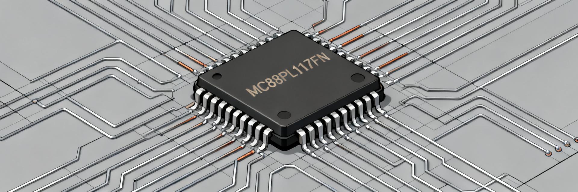
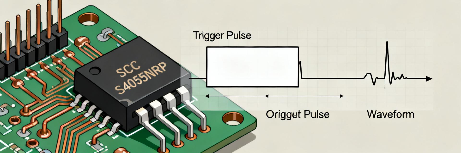
According to the MC88PL117FN datasheet, its PLL clock-driver architecture provides low-jitter frequency synthesis and multi-output clock distribution suitable for mixed-signal systems. A clear datasheet breakdown saves designers time, reduces revision cycles, and ensures correct thermal and timing margins during prototype and production phases. Product Overview & Key Takeaways The MC88PL117FN is a CMOS PLL clock driver intended to generate and distribute stable clock signals. Designers use it as a timing source feeding FPGAs, ADCs/DACs, and communication PHYs where low phase noise and multiple synchronized outputs reduce board-level jitter. MC88PL117FN PLL REF_IN Q0..Qn VCC GND (EPAD) ParameterValue (from datasheet)Test Conditions / Notes Supply Voltage Range3.0V to 3.6VNominal (3.3V) Max Supply Current (Icc)85 mA (Peak)All outputs switching @ 100MHz Output Drive / Load±24 mAVOH=2.4V, VOL=0.5V Lock Time< 10 msFrom cold-start to stable phase Thermal Limits (θJA)45 °C/WPLCC-28 Package on 4-layer PCB Deep Dive: Electrical Specifications Power Rails and Thermal Budgeting MC88PL117FN specs define absolute maximums and recommended operating ranges. Use the datasheet θJA to estimate junction temperature: Tj = Ta + (Pd × θJA). If operating at high ambient temperatures, ensure the exposed pad is stitched to a large ground plane to avoid thermal throttling. Implementation Checklist & Troubleshooting LAYOUT Place 0.1µF and 1µF decouplers within 2mm of each VCC pin. THERMAL Solder the exposed pad to a thermal land with at least 8 vias. SIGNAL Add 22Ω–33Ω series resistors on outputs for impedance matching. SymptomLikely CauseDebug Action OverheatingExceeded Pd per θJAMeasure Pd, check thermal via connectivity Unstable LockSupply noise / RippleVerify decoupling capacitors near VCC pins No OutputControl pin misstateCheck EN/SEL levels against logic thresholds Frequently Asked Questions What are the critical MC88PL117FN specs to validate in hardware? Focus validation on supply current (Iq/Icc), output drive capability under worst-case load, lock acquisition time, and thermal performance (θJA and Tj). Measure these under the datasheet test conditions and worst-case ambient/supply tolerances to ensure system margin. How should I size decoupling and thermal vias for the MC88PL117FN? Place a 0.1µF plus 1µF decoupling pair at each supply pin, within 1–2mm. Provide a soldered exposed pad with multiple thermal vias (typically 4–12 depending on board layer/copper) to reduce θJA; iterate with thermal calculations using Pd from the datasheet. Which bench tests most directly mirror datasheet curves for pass/fail? Run lock acquisition at nominal and extreme temperatures, load-step response to check output stability, and phase-noise/jitter measurements using the same load and supply conditions used in the datasheet plots. Define pass/fail thresholds from the datasheet tables. What is the primary function of the MC88PL117FN in digital systems? It serves as a low-jitter timing source to generate and distribute synchronized clock signals across digital and mixed-signal boards, feeding FPGAs and ADCs while minimizing phase noise across multiple domains.