MPM1517SJ Complete Datasheet: Specs, Pinout & Notes
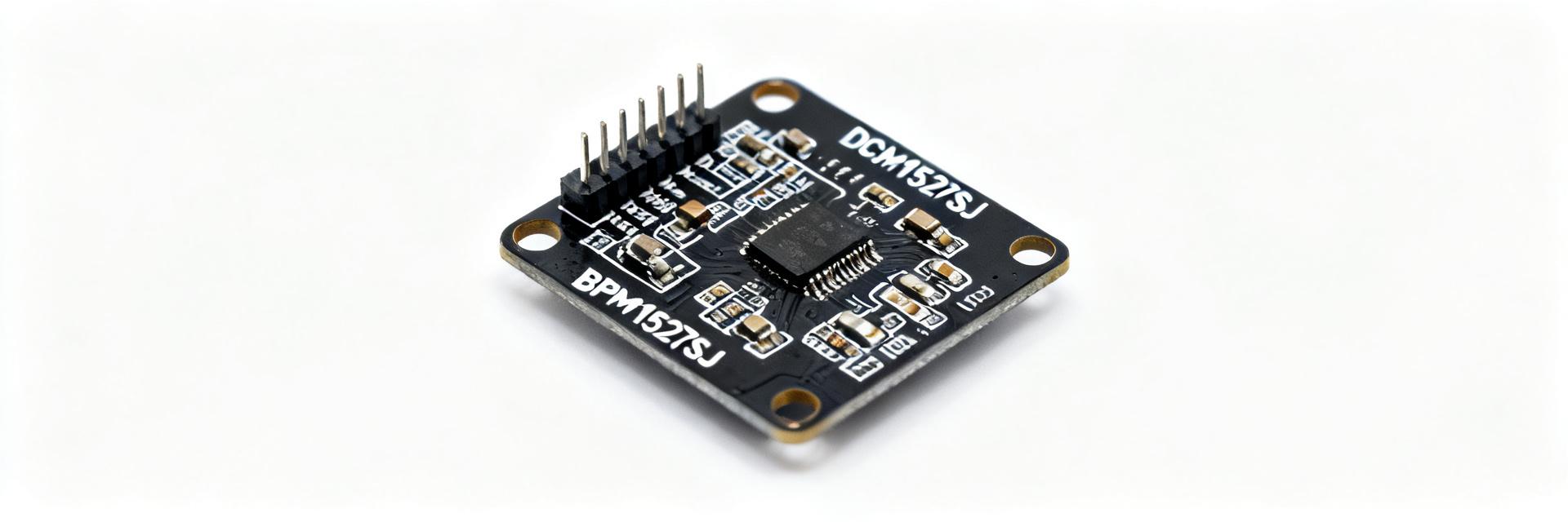
The MPM1517SJ module is a compact DC/DC power module rated for a headline output capability of 15 V at up to 1.7 A continuous from a single package. This module is ideal for regulated rails where board space and low external parts count are critical. This reference summarizes electrical limits, pinout, and practical integration tips to accelerate prototype-to-production decisions.
Overview & Key Specifications
The MPM1517SJ is a fully packaged switching regulator designed for point-of-load applications. It integrates switching elements and control circuitry, requiring only minimal external capacitors.
| Parameter | Typical / Note |
|---|---|
| Input Voltage Range | 4.5 V – 18 V (Verify absolute limits) |
| Nominal Output Voltage | 15 V (Single Output) |
| Max Output Current | 1.7 A Continuous (Thermal Limited) |
| Efficiency | 80–92% (Load/Vin dependent) |
| Switching Frequency | Internal Fixed (Refer to EMI plan) |
| Thermal Limits | Derating required above rated junction temp |
Pinout & Mechanical Details
Mapping pads correctly is essential for thermal management and signal integrity. High-current traces for VIN and VOUT should be as short as possible.
| Pin | Name | Function / Notes |
|---|---|---|
| 1 | VIN | Input supply; use low-ESR decoupling |
| 2 | GND | Power return; tie to ground plane via thermal vias |
| 3 | VOUT | Regulated 15 V output; monitor load current |
| 4 | EN | Enable input; TTL logic compatible |
| — | Thermal Pad | Connect to large copper area for heat dissipation |
Typical Circuits & BOM Highlights
A standard implementation requires minimal external components. X7R ceramic capacitors are recommended for the input to handle switching currents effectively.
| Part | Role | Notes |
|---|---|---|
| Input Cap | Decoupling | Ceramic X7R, Rated > 25V |
| Output Cap | Stability | Low-ESR, place close to VOUT pin |
| Ferrite Bead | EMI Suppression | Optional; place on VIN line |
Summary & Integration Checklist
The MPM1517SJ provides a compact 15 V solution but requires careful attention to thermal routing and decoupling. Key takeaways include:
- Headline capability: 15 V output at 1.7 A—prioritize PCB copper for continuous high-load operation.
- Layout: Follow recommended pad dimensions and place thermal vias under the module.
- Stability: Use specific low-ESR output capacitors to prevent oscillation.
- Testing: Capture switching waveforms and perform load-step tests during prototyping.