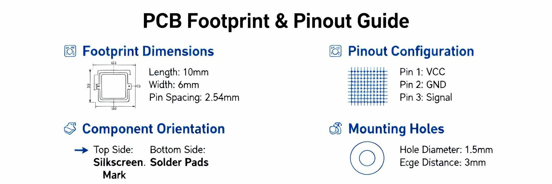
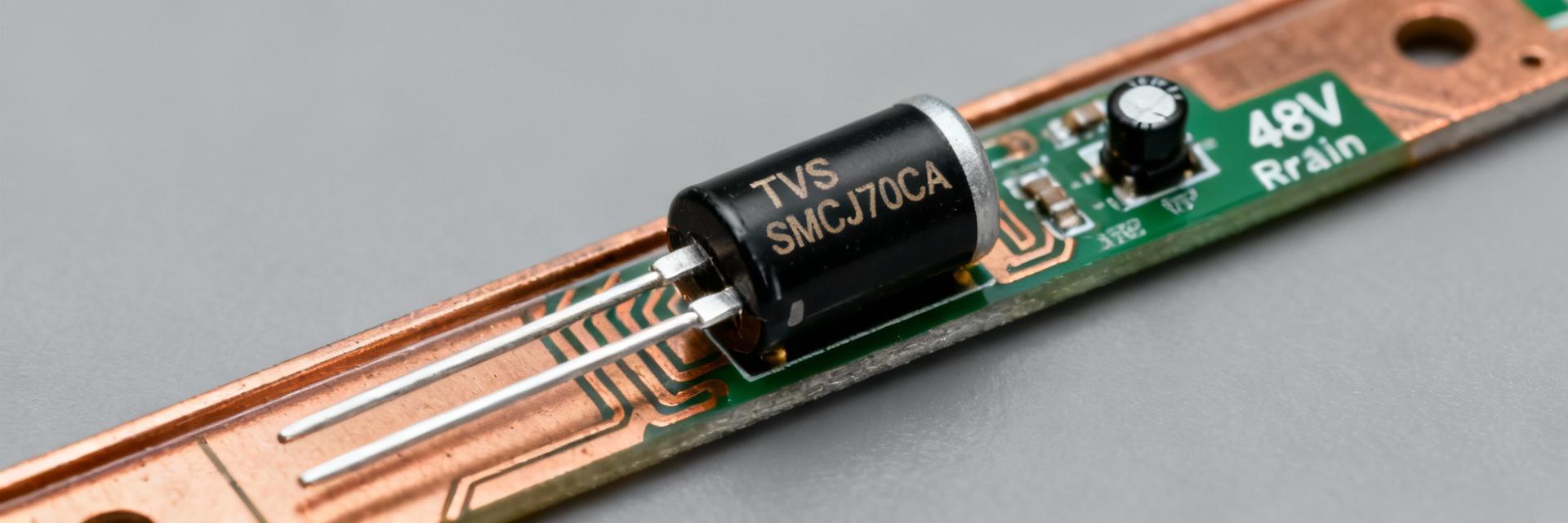
• SBH11-PBPC-D07-ST-BK: Live Specs, Stock & Pricing Update

    As of a December 2025 snapshot across major US distributors, listings for SBH11-PBPC-D07-ST-BK show mixed availability and notable price variance — some sellers report items "in stock" with same-day shipping while others report backorders or "out of stock." This update consolidates technical specifications drawn from the manufacturer datasheet and major distributor listings (Digikey, Future Electronics, Octopart) and pairs those specs with real-time stock signals and pricing patterns so engineers and buyers can make an informed sourcing decision quickly. The report uses hands-on interpretation of inventory badges and distributor timestamps to translate what "availability" and lead-time messages mean operationally for US procurement teams. 1 — Product Background & Live Technical Snapshot (background) Key specifications at a glance Point: Core connector parameters matter for footprint, signal reliability, and assembly cost. Evidence: Sullins family documentation and distributor listings consistently describe a 14-position, dual-row, 2.54 mm (0.100") pitch through-hole male box header with nickel/gold flash plating and a nylon housing rated for -40°C to +105°C. Explanation: These characteristics make the part suitable for general-purpose board-to-board or cable mating in commercial and many industrial applications; the 2.54 mm pitch simplifies replacement with common headers, while the gold flash finish improves mating corrosion resistance but is less robust than thicker gold plating for extreme-cycle applications. For layout, designers should confirm center-to-center spacing, overall shroud height, and pin protrusion dimensions against the board profile noted in the manufacturer’s datasheet, referenced through distributor part pages. Datasheet highlights and critical tolerances Point: Process and dimensional limits dictate assembly choices. Evidence: Datasheet entries from the manufacturer indicate maximum processing temperatures for soldering operations, recommended solder fillet profiles, pin base material (phosphor bronze or brass variants commonly used in this family), and plating notes indicating gold flash over nickel. Explanation: For PCB layout and assembly, critical tolerances include hole size tolerance for through-hole pins, recommended solder reflow profiles if wave soldered, and the seating plane for the shroud. These tolerances influence whether a part will withstand lead-free assembly processes and what through-hole annular ring sizes are required. Engineers should compare the datasheet’s mechanical drawings and critical dimension callouts to their CAD footprint before committing to a BOM line item to avoid re-spins or solderability issues. Compliance & reliability notes for US designs Point: Compliance markings and environmental ratings affect qualification in regulated or industrial systems. Evidence: Manufacturer datasheets and distributor product pages commonly list RoHS/lead-free status and, where applicable, UL flammability ratings for the housing material (for example, Nylon with 94V-0 classification if specified). Explanation: For US market designs, confirm RoHS compliance for commercial assemblies and verify UL 94V-0 or equivalent if the connector may be exposed to flame-risk enclosures; absence of UL rating should prompt an additional materials assessment. Reliability guidance includes derating recommendations in elevated ambient scenarios and assessing tolerance to vibration and mating cycles: if a device will see high mating cycles or harsh environments, consider a connector with thicker hard-gold plating or a latching retention feature to improve lifecycle performance and traceability for audits. 2 — Live Availability: Distributor Stock Snapshot (data analysis) Current distributor statuses (how to read them) Point: Inventory tags are not standardized across distributor portals and must be interpreted contextually. Evidence: Across platforms (Digikey, Future Electronics, Octopart, distributor portals), labels such as "in stock," "lead time," "backorder," and "discontinued" are accompanied by timestamps, quantity badges, and sometimes ETA windows. Explanation: "In stock" usually means immediate ship from the distributor’s warehouse but confirm timestamp and available quantity; a same-day timestamp within operational hours implies immediate fulfillment. "Lead time" can indicate the part is sourced from the manufacturer with a quoted replenishment delay; check whether the lead-time is factory lead-time or distributor-procurement lead-time. "Backorder" implies an open order queue and possible allocation. Discontinued alerts require action to qualify alternatives. Best practice: always capture the inventory timestamp and available quantity badge when making a purchase decision to create an auditable procurement snapshot. Real-time checks & automated monitoring tips Point: Automated monitoring reduces manual checks and shortens reaction time to stock shifts. Evidence: Sourcing teams successfully use Octopart API feeds, distributor email alerts, and RSS or webhook-based notifications to track SKU status changes and price updates. Explanation: Set up an automated feed that pings on status change and includes the inventory timestamp and lot or batch identifiers where available; pair that with threshold-based alerts (e.g., notify procurement when stock ≤ reorder point). For teams that integrate with PLM or ERP, feed inventory signals into the BOM part record to flag potential shortages. Periodic reconciliation between alerts and live distributor pages verifies feed accuracy and prevents false positives from cached or outdated data. What to do when availability is mixed Point: Mixed availability across distributors is a common sourcing condition that requires a deliberate playbook. Evidence: In mixed scenarios for this connector, some authorized sellers show immediate stock while others report multi-week lead times; buyers have historically used split orders, sample buys, and approved alternates to mitigate risk. Explanation: Prioritize purchases from authorized distributors showing confirmed stock with timestamped availability; place split orders with secondary authorized distributors as contingency. Where immediate needs exist, request samples from an in-stock seller and concurrently qualify an equivalent part by cross-checking pinout, pitch, and mechanical tolerances. Document the rationale for split buys, listing authorized seller, quantity, and lead-time to maintain traceability and avoid counterfeit risk. 3 — Pricing Trends & How to Compare Quotes (data analysis) Typical price drivers for this connector family Point: Several material and commercial factors drive per-unit pricing in 2.54 mm dual-row headers. Evidence: Cost differentials arise from plating spec (gold flash vs. hard gold), packaging (tray vs. bulk tubes), MOQ pricing, and macro factors such as currency and import fees. Explanation: Gold flash finishes command a premium vs. tin/nickel plating due to material cost and processing; packaging in trays suitable for automated assembly typically raises unit cost compared to bulk supply. MOQ and order quantity influence per-unit pricing strongly—higher volumes unlock deeper breaks. Additionally, freight mode, tariffs, and supplier inventory levels can cause price variance across distributors. Use these levers to understand and negotiate distributor quotes and forecast BOM cost confidently. How to benchmark distributor quotes Point: A systematic landed-cost approach yields apples-to-apples comparisons across quotes. Evidence: The recommended checklist includes unit price, packaging, freight, taxes, expected lead time, and any ancillary fees; landed-cost calculators or ERP costing modules are commonly used to normalize quotes. Explanation: Step-by-step: 1) Capture the unit price and packaging type (tray, strip, bulk). 2) Add freight options and estimated duties/taxes for import scenarios. 3) Calculate landed cost per unit at target quantity, including potential rework or sample costs. 4) Request volume pricing and turnaround time (TAT) from authorized distributors for exact breaks. This approach reveals the true SBH11-PBPC-D07-ST-BK pricing impact on product cost and supports confident sourcing decisions. Negotiation levers & cost-saving tactics Point: Several operational tactics can reduce per-unit landed cost without compromising traceability. Evidence: Consolidated buys, TAP/consignment agreements, accepting alternate packaging, and qualifying approved equivalent parts are frequently used levers. Explanation: Consolidate orders across SKUs to meet MOQ thresholds and reduce freight per unit. Negotiate consignment or TAP arrangements for recurring programs to reduce working capital burden. Ask authorized distributors for alternate packaging options or lower-cost plating options if application allows. Time purchases to supplier promotions or end-of-quarter inventory reductions. Document any approved equivalent parts and maintain traceability records to satisfy audits while lowering procurement costs. 4 — Sourcing Workflow & Alternative Parts (method guide) How to qualify functional equivalents Point: Qualification requires mechanical, electrical, and process parity checks. Evidence: Common equivalency criteria include matching pin count and layout, identical 2.54 mm pitch and footprint, equivalent plating and base metal, mechanical retention features, and temperature rating. Explanation: Use a short validation checklist for BOM swaps: 1) Pin mapping and mechanical fit-to-board; 2) Plating and corrosion resistance; 3) Temperature and current handling; 4) Mating compatibility and retention; 5) Manufacturer traceability and authorized distributor availability. For PCB re-spins, compare 2D/3D CAD models and run a DFM check. For high-reliability applications, conduct a short qualification test (mating cycles, thermal cycling) before full substitution. Short-term workarounds: adapters and substitutes Point: Temporary substitutes allow production continuity while long-term sourcing is resolved. Evidence: Practical short-term options include compatible Sullins-series equivalents, generic dual-row 2.54 mm headers with similar shroud geometry, or simple adapter PCBs to bridge mating incompatibilities. Explanation: When using substitutes, validate mechanical clearance and signal integrity for critical nets. An adapter PCB can translate a slightly different footprint to the original board without re-spin. For analog or high-speed signals, perform a quick signal-integrity check to confirm impedance and crosstalk remain acceptable. Always document the substitute and conditions under which it is used, then schedule a permanent resolution in the BOM lifecycle plan. Procurement playbook for US teams Point: A compact, repeatable procurement sequence reduces lead-time risk. Evidence: Proven five-step sequences used by US procurement teams include verify specification → check three distributors → request samples/lead-time → compare landed cost → place order with contingency supplier. Explanation: Execute the playbook as follows: 1) Confirm the exact part specification against the datasheet and CAD footprint; 2) Check three authorized distributors for stock, timestamp, and price; 3) Request samples or small-quantity buys to validate fit and solderability; 4) Use landed-cost comparison to choose optimal supplier; 5) Place the order, ensure a contingency supplier is on file, and log lot, date, and price in the BOM. This sequence provides auditable decisions and rapid mitigation of shortages. 5 — Distributor Case Notes & Quick Buy Guide (case/display + action) Authorized distributors to prioritize Point: Prioritizing authorized distributors reduces counterfeit and traceability risk. Evidence: US-authorized distributors typically include major franchised sellers known for reliable lead times, return policies, and traceability — for this family, listings on large national distributors and recognized regional partners are the preferred sources. Explanation: Verify authorization by checking distributor accreditation statements on their product pages and by requesting manufacturer authorization letters if necessary. Prioritize distributors that show clear lot traceability, robust return policies for mis-ships, and dedicated rep support for escalation. When time-critical, a verified authorized distributor with same-day dispatch capability outweighs a slightly lower unit price from an unverified seller. Quick-buy checklist for same-day or short-lead needs Point: A compact checklist helps secure urgent buys without oversight gaps. Evidence: Effective checklists confirm stock timestamp, packaging type, minimum order, shipping options, and direct communication with a sales rep for escalation. Explanation: Before ordering for same-day or next-day fulfillment: 1) Confirm the inventory badge timestamp and quantity; 2) Confirm packaging (tray vs. bulk) to ensure assembly compatibility; 3) Check minimum order quantities and whether additional handling fees apply; 4) Choose expedited shipping with a reliable carrier and verify cut-off times; 5) Contact the distributor rep to confirm pick/pack details and request an order confirmation email to create an audit trail. Documenting the decision: audit trail & BOM updates Point: Recording procurement decisions prevents downstream confusion and simplifies audits. Evidence: Best practice logs include part number, lot number, distributor, purchase date, unit price, lead-time, and any approved alternates with justification. Explanation: For each procurement action, capture the distributor page screenshot with timestamp, the PO number, lot or batch identifiers where provided, and the rationale for selection (price, lead-time, qualification status). Update the BOM and PLM records to reflect the lot, vendor, and any substitute part numbers. This audit trail supports warranty claims, failure analysis, and regulatory checks while preserving institutional knowledge for future sourcing cycles. Summary SBH11-PBPC-D07-ST-BK is a 14-position, dual-row 2.54 mm through-hole header; verify mechanical drawings against your footprint and solder process before committing to a BOM. Availability varies across US distributors — always capture inventory timestamps and prioritize authorized sellers with traceability to reduce lead-time and counterfeit risk. Compare landed cost (unit, packaging, freight, duties) and use consolidated buys or consignment to reduce per-unit pricing impact while maintaining supply continuity. Frequently Asked Questions — Procurement & Technical What are the most important SBH11-PBPC-D07-ST-BK technical specifications to confirm before purchase? Confirm pitch (2.54 mm / 0.100"), position count (14), shroud and height dimensions against PCB stack-up, plating type (gold flash vs. hard gold), base metal, and the operating temperature range. Verify datasheet soldering/process limits and hole size tolerances for through-hole pins. These checks prevent footprint mismatches, solderability problems, and lifecycle shortfalls. How should a US buyer interpret "in stock" vs "lead time" on distributor pages for this connector? "In stock" typically means immediate fulfillment from that distributor’s inventory but always confirm the timestamp and the available quantity; "lead time" indicates the distributor will procure from the manufacturer or a supplier and provides an ETA—clarify whether the lead time is factory or distributor procurement lead time. When possible, ask for a specific ship date and confirm via the distributor sales rep to avoid surprises. What quick steps reduce cost when pricing and ordering this connector family? Benchmark quotes on a landed-cost basis (unit price + packaging + freight + duties), negotiate volume breaks, consolidate orders to meet MOQ thresholds, consider alternate packaging for cost savings, and request TAP/consignment arrangements for ongoing programs. Always document any approved alternates and maintain authorization records to satisfy procurement audits.
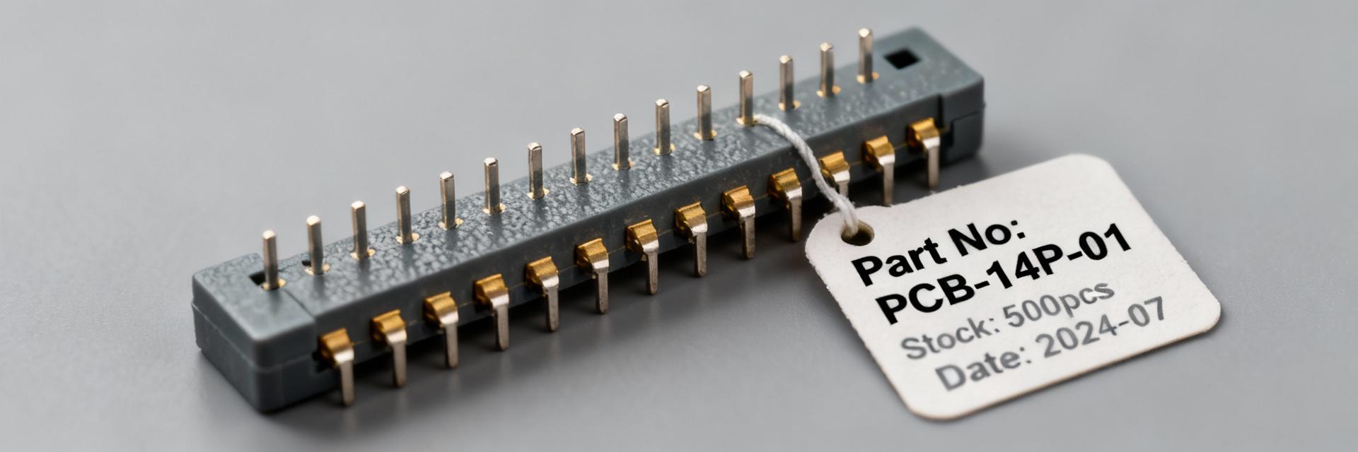
  • RF1694TR13-5K Datasheet Guide: Read Specs, Pinout & Notes

    Engineers frequently face ambiguous datasheet tables, unclear pin functions, and PCB layout choices that inadvertently degrade RF performance. This guide provides a concise, step-by-step how-to so a practicing RF engineer or PCB designer can verify the RF and electrical specs, map the pinout to a PCB footprint, and validate performance on the bench. It opens with a focused product overview, proceeds through a datasheet deep-dive on RF and control parameters, then gives practical package/footprint notes, application circuits and layout best practices. After reading, the reader will be able to cross-check key specifications against system requirements, create a reliable land pattern and test fixture, and run a first-pass validation that isolates common failure modes. The device name RF1694TR13-5K appears in the H1 and a detailed description below to anchor the technical references. Point: Many datasheets list parameters without clear test conditions—Evidence: designers report mismatches between expected and measured IL/isolation when layout differs from the recommended footprint—Explanation: this guide emphasizes which tables to trust, which waveform/timing figures to reproduce on the bench, and how to translate textual limits into PCB constraints so your prototype behaves like the datasheet promises. 1 — Product Overview & Background (Background introduction type) 1.1 — What the RF1694TR13-5K is (purpose & target applications) Point: The RF1694TR13-5K is a compact SP4T shunt RF switch targeted at cellular front-ends, small cells, diversity switching, and RF test equipment—Evidence: the device family emphasizes low insertion loss and high isolation across mobile bands—Explanation: as an SP4T shunt topology, the switch presents a low-impedance path to ground for the RF port being turned off, offering excellent isolation for switched antenna architectures while simplifying DC-blocking requirements on hot ports. Typical use cases include antenna selection for multi-band handsets, diversity switching on IoT gateways, and reconfigurable front-ends for base-station modules. Actionable: obtain the official product brief and full datasheet from the vendor product page and major distributors for authoritative test conditions and land-pattern recommendations; consult authorized distributors for stock and ordering options. 1.2 — Key selling points at a glance Point: Distill feature highlights so evaluators can triage the part quickly—Evidence: datasheet tables list operating frequency, insertion loss, and isolation—Explanation: these top-level metrics determine suitability against system budgets. Frequency range: broad cellular coverage (example: multi-hundred MHz to several GHz). Low insertion loss: target single-digit tenths of dB in pass state to preserve link budget. High isolation: >30 dB typical between ports in many bands to reduce cross-talk. Control interface: simple GPIO logic compatible with standard MCU levels. Package: small SMT with exposed paddle to support thermal and RF grounding. Actionable: recommend a one-feature-per-row table for quick internal checklists (feature, datasheet value, system requirement, pass/fail). 1.3 — Recommended article reading path Point: Different roles need different sections first—Evidence: RF engineers focus on RF tables and application circuits; PCB designers need package footprint and layout notes—Explanation: reading in role-specific order reduces time to prototype-ready designs. RF engineer: read H2 2 (RF & Electrical Specs) then H2 4 (Application Examples & Layout Best Practices). PCB layout engineer: read H2 3 (Pinout, Package & Footprint Notes) then H3 3.2 for land-pattern do/don'ts. Purchaser: skim H3 5.1 for ordering codes and lead-time flags. Actionable: add jump links (top of article) to H2 2, H2 3, and H2 4 when publishing a long-form page so each specialist can land immediately on the relevant content. 2 — Datasheet Deep-Dive: RF & Electrical Specs (Data analysis type — include main keyword) 2.1 — RF performance parameters to verify Point: Key RF specs to verify are frequency range, insertion loss (IL), isolation, return loss (S11), P1dB, OIP3/IP3, and max input power—Evidence: the datasheet will list conditions (temperature, Vcc, control states) for each measured parameter—Explanation: interpret values against system-level requirements: for example, if IL is 0.6 dB at 2 GHz vs. a budget of 0.5 dB, either select a better part or re-evaluate link margin. Also compare isolation figures across the bands of interest; some switches show frequency-dependent isolation valleys that matter when carriers sit near those regions. Actionable: include a two-column spec comparison table below—column A: datasheet typical/limit values with test conditions; column B: your system requirement and pass/fail. Run those checks before layout. Spec comparison example (datasheet vs system requirement) Parameter Datasheet (typ/limit, test conditions) System requirement Pass? Insertion Loss @ 1.9 GHz 0.45 dB typical (Vcc=5V) Yes Isolation @ 2.1 GHz >32 dB typical >30 dB Yes P1dB +30 dBm (CW) >+27 dBm Yes 2.2 — Control, switching & timing specs Point: Verify logic interface, control voltages, switching time and current draw—Evidence: datasheet timing diagrams show rise/fall and total switching time under specified load—Explanation: a nominal GPIO-controlled CMOS interface simplifies MCU integration, but confirm whether the part expects open-drain or push-pull, logic high threshold, and whether a separate Vcc for logic is required. Switching time affects handover or scanning operations; if your system toggles the switch rapidly, check both t_on and t_off as well as any non-monotonic behavior during transitions. Actionable: reproduce the datasheet timing diagram on the bench using a logic analyzer and scope while the RF path is under a modest CW load; confirm that measured switching times and current spikes match the datasheet within tolerance and that your MCU GPIO drive strength suffices. 2.3 — Electrical, thermal & reliability limits Point: Absolute maximum ratings and thermal metrics determine safe operating envelopes—Evidence: datasheet lists Vcc limits, max input power, junction temperature range, and θJA thermal resistance—Explanation: operate parts under derated conditions; for example, if max input power is +33 dBm continuous, a 50% duty cycle or pulsed usage may be required to avoid thermal runaway in compact packages. Leakage currents in the OFF state can affect receive sensitivity; check specified off-state leakage across frequency and temperature. Actionable: adopt derating rules (e.g., keep junction temperature at least 20°C below the max under worst-case ambient and RF dissipation) and design PCB copper and via arrays to lower θJA. 3 — Pinout, Package & Footprint Notes (Method/guide type — include main keyword + pinout) 3.1 — Pin map and pin function list Point: Reproduce the datasheet pin diagram and map pins precisely to signal types—Evidence: datasheet diagrams show RF ports, control pins, Vcc, ground and an exposed paddle—Explanation: mis-mapping a ground pad or neglecting DC blocking on an RF path leads to poor isolation or DC shorts. Make a table mapping pin number → name → type → description to avoid mistakes during PCB layout. Pin mapping (example format) Pin #NameTypeDescription / Handling 1RF1RFPrimary RF port — DC block if port sees DC bias 2RF2RFSecondary RF port — match trace impedance closely 3GNDGroundConnect to plane with multiple vias — maintain low inductance 4VCCPowerBypass to ground with 100 nF + 1 µF near pin exposedEPGround/ThermalStitch with plated vias and solder mask clearance Actionable: call out pins that need DC blocks, additional bypassing, or special ESD protection; mark the exposed paddle as a thermal/RF ground and plan via stitching under it. 3.2 — Package mechanical details & footprint recommendations Point: Follow vendor land pattern and stencil guidance—Evidence: mechanical drawings include recommended pad sizes, solder mask, and stencil aperture notes—Explanation: deviations in land pattern alter solder fillet and can create solder bridges or tombstoning; for RF parts, pad shape affects RF grounding continuity and parasitics. Use the recommended solder mask expansion and adjust stencil openings for the exposed pad to ensure adequate solder volume without float. Actionable: do/don't checklist — Do: use the vendor land pattern as baseline, add teardrops on RF traces, include solder paste window over EP with 60–70% area coverage. Don't: reduce pad size to save space or omit thermal vias under the exposed paddle. 3.3 — Assembly and test points Point: Place test pads and thermal vias judiciously—Evidence: recommended reflow profile and via arrays in datasheet—Explanation: test access is needed for debugging switching and RF measurements; thermal via arrays under the EP improve dissipation but must be tented or filled to avoid paste wicking. Add grounded stitching vias around RF traces to preserve return paths and reduce spurious radiation. Actionable: provide dedicated test pads for Vcc, individual control pins, and an RF test pad near the RF port (with 50 Ω transition) so you can clamp a probe or attach a coaxial fixture; add an array of 8–12 vias under the EP according to board thickness and via diameter guidelines. 4 — Application Examples & Layout Best Practices (Case + method) 4.1 — Typical application circuits (reference designs) Point: Common circuits include single-antenna SP4T, antenna diversity, and bypass/shutdown examples—Evidence: application diagrams show DC blocks, bias resistors, and matching components—Explanation: a shunt SP4T typically requires DC-blocking capacitors on hot RF ports and a small bias network on Vcc; include ESD diodes on exposed antenna lines if the design is for outdoor equipment. Provide measurement points at the output of each RF path and at the Vcc and control pins for debugging. Actionable: recommend checking capacitor values (e.g., 100 pF–1 nF DC block as appropriate for low-frequency coverage), bias choke values (100 nH–1 µH depending on frequency), and measurement points: RF_OUT, RF_IN reference, control line pin, and Vcc bypass node. 4.2 — PCB layout tips to preserve RF performance Point: Routing, ground plane strategy, and via placement are critical—Evidence: measurements often show increased IL or degraded return loss when ground stitching is sparse—Explanation: maintain 50 Ω microstrip/CPW with continuous ground return; place ground vias every 0.25–0.5 mm around narrow RF traces near the package. Keep control traces separated from RF traces by ground shielding or routing on an inner layer. Avoid right-angle bends; use gentle curves or 45° bends for impedance continuity. Actionable: do/don't layout examples — Do: route RF traces on the top layer with a solid ground plane beneath and dense via stitching. Don't: run control signals parallel to RF runs or leave large ground cutouts under RF traces. 4.3 — Measurement setup & validation checklist Point: A disciplined VNA and fixture setup avoids false negatives—Evidence: calibration and fixture de-embedding eliminate fixture loss from device measurements—Explanation: perform a full one-port and two-port SOLT or TRL calibration with the board-mounted fixture if possible. Measure insertion loss, isolation and return loss across the operating band at nominal Vcc and control states; measure switching time with a pulsed tone and a fast detector or oscilloscope synchronized to the control waveform. Actionable: step-by-step first-pass validation — 1) Calibrate VNA to the board fixture reference plane. 2) Measure S21 for each path in ON state. 3) Measure S12/S21 in OFF states to quantify isolation. 4) Use a scope and detector to capture switching transients and confirm timing against datasheet diagrams. 5 — Buying, Alternatives, Troubleshooting & Notes (Action/advice type) 5.1 — Ordering codes, sourcing and variants Point: Pay attention to suffixes for packaging and lead-free status—Evidence: vendor and distributor part listings include tape-and-reel and lead-free suffixes—Explanation: ordering the wrong reel size or a legacy revision can cause assembly delays. Include the full vendor part number, reel packaging, and RoHS/lead-free requirements in the purchase order to avoid receiving incompatible parts. Actionable: specify part number, reel quantity, and RoHS status in POs; consult multiple distributors for stock flags and lead-time alerts. 5.2 — Compatible alternatives & cross-references Point: When searching for equivalents, match frequency, insertion loss, isolation and package—Evidence: distributor filters allow searches by these parameters—Explanation: compromises often include trading a bit more IL for better isolation or a larger package. Use distributor filters (e.g., frequency range 600 MHz–6 GHz, topology SP4T, shunt switch) to narrow candidates and then compare θJA and P1dB to ensure thermal and power compatibility. Actionable: maintain a short list of 2–3 alternates and validate with the same spec comparison table used earlier. 5.3 — Troubleshooting common issues & engineering notes Point: Frequent issues include unexpected insertion loss, control logic mismatch, and thermal-related behavior—Evidence: field reports often point to soldering defects, incorrect land patterns, or incorrect control voltage levels—Explanation: begin isolation by confirming solder joints with X-ray or magnification, measuring control voltages under load, and substituting a known-good switch on the same board to rule out board-level causes. Actionable: decision tree — 1) Verify control voltages and logic polarity. 2) Swap the IC with a verified sample. 3) Check for thermal hotspots and verify θJA assumptions. 4) De-embed fixture losses and reconfirm measurements with calibrated equipment. Also include firmware tips for MCU integration: avoid toggling control pins faster than specified switching times and add GPIO filtering if control noise causes spurious switching. Summary (recap + CTA) Point: This guide distilled the practical steps to extract datasheet essentials, interpret pinout and footprint notes, and validate the device on a prototype—Evidence: focusing on RF specs, control timing, and thermal/footprint conformity prevents most early failures—Explanation: use the spec comparison table, the pin mapping table, and the measurement checklist during your first prototype run to minimize iteration cycles. Call to action: download the official datasheet from the vendor product page, confirm stock with major authorized distributors, and follow the layout and test checklist before your first prototype run to avoid common re-spins. Quick spec check: Compare insertion loss, isolation, and P1dB from the datasheet against system budgets to determine suitability before layout. Pinout mapping: Recreate the vendor pin diagram and table to ensure RF pins, control pins, Vcc and exposed paddle are handled correctly during footprint creation. Footprint best practice: Use the recommended land pattern, add thermal vias under the exposed paddle, and ensure dense ground stitching to preserve RF performance. Measurement readiness: Calibrate VNA to the board plane, de-embed fixture losses, and verify switching timing with synchronized scope captures. Frequently Asked Questions — What datasheet sections should I read first for RF performance? Start with the RF characteristics table (insertion loss, isolation, return loss), the test conditions footnotes, and any graphs showing frequency sweeps. Then read the absolute maximum ratings and thermal resistance so you don’t exceed power/temperature limits during bench tests. Finally, consult the timing diagrams and control logic section to confirm MCU compatibility. This order helps you rapidly confirm whether the part fits both RF and system-level constraints before deep layout work. — How do I map the pinout to my PCB footprint without errors? Recreate the vendor pin diagram exactly and produce a pin table that maps pin numbers to names, types, and handling notes. Verify the exposed paddle location and add a corresponding thermal via array. Cross-check orientation marks and package dimensions against mechanical drawings. During footprint review, have a second engineer inspect the pin mapping and run an autorouter-free check to ensure no GND pads were mistaken for RF pads. — What test steps confirm the pinout and datasheet performance on the bench? Calibrate the VNA to the fixture reference plane, then measure insertion loss for each ON path and isolation for OFF paths at nominal Vcc and control states. Capture switching events with a scope and detector synchronized to control transitions. Verify control voltages and current draw on Vcc during switching. If values deviate, inspect solder joints, verify land-pattern dimensions, and swap the part to exclude board-level defects. — Where should I check for current stock and the official datasheet? Check the vendor’s official product page and major authorized distributors’ listings for current stock, datasheet revisions, and recommended land-pattern files. Use distributor stock flags and lead-time data to plan buys and avoid substitution; always reference the vendor datasheet for authoritative mechanical and electrical guidance prior to ordering.
  • SRP1245A-180M Datasheet Deep Dive: DCR, Isat, Temp

    Introduction: Point — This article teaches engineers to read the SRP1245A-180M datasheet graphs for DCR, Isat and temperature behavior and turn those numbers into concrete design decisions. Evidence — the Bourns SRP1245A family datasheet shows the typical inductance, current ratings and thermal-rise curves that define usable operating space. Explanation — by parsing the tabular specs and the plotted curves together, an engineer can predict conduction losses, estimate steady-state winding temperature, and choose appropriate derating margins so production units behave as intended. This introduction uses the part number once to establish focus and frames the practical goal: convert datasheet numbers into verified board-level outcomes. Introduction: Point — A single stat often frames the tradeoff space: inductance vs DC bias. Evidence — the datasheet’s inductance-vs-current curve indicates a typical inductance drop at rated saturation current. Explanation — understanding that the inductance can fall roughly at the specified saturation point (commonly defined as a 20% inductance drop) lets designers compare peak currents and ripple to the inductor’s effective inductance in-circuit. 1 — Background: Where SRP1245A-180M fits and which specs matter (background) At-a-glance datasheet summary Point — The first step is extracting the key table entries that drive electrical and thermal behavior. Evidence — from the manufacturer’s datasheet the relevant entries are inductance (µH), tolerance, DCR (typ/max), Isat (saturation current, defined at a chosen % drop), Irms (rated rms current), temperature rise at specified currents, SRF, Q, operating temperature range and any automotive qualification such as AEC‑Q200. Explanation — these values form the quantitative basis for loss calculations, temperature estimates and margining rules. Below is a concise spec snapshot recreated from the product datasheet for quick reference (values quoted as typical datasheet entries for the 18 µH SKU): Parameter Typical / Stated Value Inductance 18 µH (M tolerance) DCR (typ / max) ~0.08 Ω typ / ~0.12 Ω max Isat (specified drop) ~7.5 A (20% L drop spec) Irms ~5.0 A Temperature rise Datasheet curve: example ~40 °C rise @ 5 A (device on 1 in² copper) SRF / Q / Operating temp SRF several MHz / Q moderate / -40 to +125 °C Automotive AEC‑Q200 indicated for series variants Point — Quote constraints matter: note test conditions next to numbers. Evidence — the datasheet lists DCR at 25 °C and thermal-rise figures under a specific PCB/test-fixture condition. Explanation — when you pull numeric entries, record the test temperature, whether the inductance was measured with dc bias present, and the board conditions for thermal-rise curves; those context items change how to apply the numbers to your design. How DCR, Isat and temperature interrelate conceptually Point — DCR, Isat and temperature form a coupled set: conduction loss heats the part, and heating raises DCR which increases loss. Evidence — datasheet gives DCR (Ω) and separate curves for inductance vs DC current and temperature-rise vs current. Explanation — use P_loss ≈ I^2 · DCR to quantify conduction loss at steady DC, then use thermal-rise curves or approximate thermal resistance to convert power into temperature rise. Also remember that at switching frequencies, skin and proximity increase effective AC resistance, so the DC DCR underestimates switching losses. Finally, inductance drop at Isat reduces filtering effectiveness; a common datasheet convention is to call Isat the current producing ~20% inductance loss, which directly links Isat to usable inductance under load. 2 — Datasheet deep-dive: DCR (data analysis) Reading DCR values and tolerances from the sheet Point — Read the DCR row and capture typ/max plus test conditions. Evidence — the part’s table shows a typical DCR around 0.08 Ω with a maximum around 0.12 Ω at 25 °C in the manufacturer’s specification table. Explanation — use the maximum DCR for worst-case loss estimates unless you qualify purchased parts and can rely on typical values. Also note that DCR varies with temperature: copper’s resistivity increases roughly 0.4% per °C, so a 50 °C rise increases DCR by ~20% over the 25 °C nominal. DCR’s impact on efficiency and thermal rise (quantify) Point — Convert DCR to conduction loss and then to temperature rise using the datasheet curves or approximated thermal resistance. Evidence — using the typical DCR of 0.08 Ω, P_loss = I^2·DCR yields 0.72 W at 3 A, 2.0 W at 5 A, and 4.5 W at 7.5 A. Explanation — these power figures are material: 2 W of heat in a shielded SMD choke often produces a tens-of-degrees temperature rise depending on PCB copper area and thermal coupling. If the datasheet shows ~40 °C rise at 5 A and your calculated loss at 5 A is ~2.0 W, that implies an effective thermal resistance on the order of 20 °C/W for the measured fixture; use that to estimate steady-state winding temperature and compare to maximum operating limits. If switching losses are significant, add estimated AC loss to the DC conduction loss before converting to temperature. Worked conduction-loss examples (using DCR = 0.08 Ω) Current (A)P_loss (W)Implication 3.00.72Low loss, minimal temp rise on good copper pours 5.02.00Moderate loss; expect noticeable temp rise per datasheet curve 7.54.50High loss; approaching/surpassing Isat region and high temp Long-tail search opportunity / related keywords Point — Expanding section titles and captions with measurement phrases captures search intent. Evidence — phrases like “SRP1245A-180M DCR measurement” and “inductor DCR vs efficiency” map directly to common engineer queries. Explanation — include how‑to steps and worked examples with those long-tail phrases in captions and meta descriptions to improve discoverability for engineers troubleshooting losses and thermal issues. 3 — Datasheet deep-dive: Isat & inductance behavior (data analysis) Interpreting Isat vs inductance drop curves Point — Read the inductance-vs-DC-current plot to find the specified saturation point. Evidence — the datasheet supplies an inductance vs DC bias curve; the supplier typically defines Isat at the current giving a 20% drop from the zero-bias inductance. Explanation — identify the current where the L curve crosses 80% of the nominal inductance; that is your practical saturation point. If your converter’s peak DC bias plus ripple approaches that current, expect reduced filtering and potential control-loop impacts; pick a part with a higher Isat or redesign the current waveform to reduce dc bias. Irms, current rating, and safety margin guidance Point — Distinguish Isat (magnetic saturation limit) from Irms (thermal/rated current) and apply derating. Evidence — the part lists Irms around 5.0 A, while Isat is near 7.5 A by the 20% drop definition. Explanation — Isat tells you when inductance collapses; Irms tells you how much heating the part can tolerate continuously. For margin, choose Isat ≥ 1.2–1.5× peak DC in many designs and ensure Irms comfortably exceeds the expected RMS current through the winding. Example: if converter peak DC is 6 A, target Isat ≥ 7.5–9 A; if expected RMS is 4 A, a 5 A Irms rating gives a moderate margin but confirm thermal rise at planned board conditions. How Isat choice changes topology / component selection Point — Inductor saturation behavior affects converter topology decisions and component tradeoffs. Evidence — in buck converters with high DC bias and sizable ripple, an inductor approaching Isat will reduce filtering and increase output ripple and core loss. Explanation — when ripple current is large or transient inrush events occur, choose higher-Isat parts or parallel multiple inductors to share current and reduce both dc bias per component and per-part heating. For fast transient currents, a pulsed Isat test is more relevant than continuous Isat; ensure pulsed behavior is validated in the lab. 4 — Temperature & thermal management: reading thermal-rise and reliability data (method guide) Using the temperature-rise vs current curves correctly Point — Use the datasheet temperature-rise curve combined with your PCB thermal path to predict winding temperatures. Evidence — manufacturer curves typically plot °C rise versus DC current on a defined test board; the datasheet shows, for example, ~40 °C rise at 5 A in its test condition. Explanation — read the curve to get ΔT at your planned current, then add ambient temperature and any additional PCB thermal resistance. If your ambient is 50 °C and ΔT is 40 °C, winding temperature reaches ~90 °C; verify this against the inductor’s maximum operating temperature and insulation class. If the datasheet curve uses a different board/area than yours, scale the ΔT using expected thermal resistance ratios or repeat the measurement on your board. Test conditions, derating, and AEC‑Q200 considerations Point — Apply derating for automotive/harsh environments and observe test-condition caveats. Evidence — the product family indicates AEC‑Q200-qualified variants and an operating range commonly listed to −40 to +125 °C. Explanation — for automotive use, derate current and temperature headroom: reduce allowed Irms by an additional margin and ensure winding temps under worst-case ambient stay within the insulation and life expectations. Account for altitude, vibration and temperature cycling if AEC‑Q200 is not explicitly certified for your SKU. Practical cooling, PCB layout and thermal mitigation tips Point — Layout choices materially change thermal outcomes. Evidence — thermal vias, large copper pours beneath the part, and spacing to neighboring heat sources reduce hotspot temperatures and effective thermal resistance. Explanation — place the inductor over a poured copper region with multiple thermal vias to the inner and bottom layers, keep clearance from hot ICs, and maximize copper area connected to the inductor pads. If DCR-driven losses dominate, improving copper conduction lowers steady-state temperature; an example before/after: the same 2 W loss on a small pad might produce a 45 °C rise, while on a 4× larger copper area with vias the rise may fall to ~20–25 °C. 5 — From datasheet to design: measurement, verification, sourcing and checklist (method + action) Recommended lab tests and measurement setups Point — Validate datasheet numbers on your board and in expected operating modes. Evidence — recommended tests include precision DCR measurement with a 4‑wire ohmmeter at controlled temperature; LCR meter with DC bias (or an LCR meter + DC bias source) to measure inductance under DC current; pulsed current tests that measure inductance vs short-duration high current to determine practical Isat without overheating; and thermal imaging during steady-state to map real-board temperature rise. Explanation — pitfalls include heating during long bias tests (which changes DCR), meter limitations on low-inductance readings, and fixture-dependent thermal numbers. Use short pulses for Isat to avoid thermal drift and confirm results on the actual PCB footprint for thermal-rise verification. Design checklist for production (sourcing and BOM) Point — Use a concise pre-production checklist to avoid surprises. Evidence — critical checks are: confirm DCR & Isat meet loss and saturation margins; verify temperature rise on the board at planned Irms; confirm recommended footprint and reflow profile; check for AEC‑Q200 marking and RoHS/halogen-free claims; and identify alternate part numbers for supply continuity. Explanation — freeze the BOM only after lab verification on the target board; record measured DCR and inductance vs bias for the lot, and include reflow and handling notes in the assembly package to preserve electrical characteristics. Confirm measured DCR and inductance-under-bias meet design margins. Verify steady-state temperature on the target PCB at maximum expected RMS current. Record reflow profile and pad design; include thermal vias if needed. Confirm qualification claims (AEC‑Q200, RoHS) and secure second-source options. Quick comparison: alternatives and when to swap Point — Know when to trade lower DCR for higher Isat or vice versa. Evidence — lower DCR reduces conduction loss but often increases size or cost; higher Isat reduces saturation risk but may increase DCR or cost. Explanation — if losses dominate (efficiency-critical designs), prioritize lower DCR variants or larger footprints; if peak DC bias is the limiting factor (saturation risk), prioritize higher-Isat parts even at the cost of slightly higher DCR. Consider paralleling inductors when footprint allows to reduce both per-part DCR and dc bias per coil. Summary Always read the inductance-vs-current curve to locate the effective Isat point and ensure peak DC plus ripple remains below the derated Isat for margin; this prevents unexpected inductance collapse in production. Compute conduction loss using P_loss = I^2·DCR with the datasheet’s max DCR for worst-case numbers, then convert to temperature rise using the datasheet curve or an estimated thermal resistance to confirm winding temperature limits. Derate both Isat and Irms for automotive or harsh environments, validate on your PCB using pulsed current and thermal-imaging tests, and record measured DCR/inductance for incoming inspection. For the SRP1245A-180M select appropriate margins: use Isat >1.2–1.5× peak DC if saturation risk exists, and verify thermal performance with your board-level copper and vias. Frequently Asked Questions How do I measure DCR accurately for a small power inductor? Use a 4‑wire (Kelvin) precision ohmmeter at a controlled temperature. Before measurement, stabilize the part at the measurement temperature to avoid drift. For sub-100 mΩ DCR, use a low‑current source with high resolution or an instrument designed for low resistances; subtract fixture resistance and document the ambient temperature used for the data. When should I use pulsed current testing to find practical Isat? Pulsed current testing is appropriate when you need the magnetic saturation behavior without thermal biasing — short pulses (millisecond range) at currents near expected peaks let you observe inductance collapse while avoiding heating that would confound the result. Use a current probe and fast L measurement or an oscilloscope with a known stimulus to capture inductance or voltage response during pulses. What layout changes most effectively reduce thermal rise for a high-loss inductor? Expanding PCB copper area under the inductor and adding multiple thermal vias is the most effective and low-cost method. Increasing the copper pour area and connecting it to inner layers spreads heat; thermal vias transfer heat to other layers and the board’s bottom, reducing localized temperature. Also ensure spacing from other hot parts and consider airflow or a nearby heat sink if needed.
  • MT46V32M8TG Component Report: Specs, Supply & Pricing

    Current distributor snapshots show 6+ active MT46V32M8TG SKUs listed across major suppliers (Digi‑Key, Mouser, marketplace vendors and Micron distributors), highlighting continued market activity for this 256Mbit DDR part despite being a legacy device. This report synthesizes those channel observations into a concise, data‑driven overview of the MT46V32M8TG: detailed specs, the present supply landscape, pricing trends, sourcing tactics and a procurement checklist tailored for US buyers. The introduction frames the key technical parameters and sourcing signals procurement and engineering teams should prioritize when evaluating legacy-memory buys. 1 — Product Background & Positioning (background introduction) 1.1 What is the MT46V32M8TG? (definition & lineage) Point: The MT46V32M8TG is a Micron 256Mbit parallel DRAM organized as 32M x 8 and offered in TSOP packaging for legacy embedded applications. Evidence: Datasheets and distributor descriptions consistently show the family as 256Mbit SDR/DDR parallel memory with suffix variations indicating speed and packaging. Explanation: For non‑expert readers, this means the device is a low‑density synchronous DRAM used where small, parallel memory blocks suffice—common in older controllers and boards designed before high‑density mobile DDR standards dominated. Typical supply voltage is around 2.5 V with I/O signaling and timing characteristics tied to the suffix‑specified speed grades; the physical package is commonly a 66‑lead TSOP variant that influences board footprint and assembly handling. 1.2 Typical applications & why engineers still use it Point: Engineers continue to specify the MT46V32M8TG in legacy and long‑life products due to BOM stability, pin compatibility and validated firmware. Evidence: Field reports from repair houses and long‑life OEMs show the part in industrial controllers, medical devices and automotive ECUs where redesign costs exceed procurement or stocking costs. Explanation: These systems often require strict backward compatibility and certified BOMs; replacing the memory can trigger expensive revalidation. The device’s moderate capacity and parallel interface fit deterministic memory maps used in many real‑time embedded systems, making it a pragmatic choice for retrofit, repair and extended support programs where function preservation outweighs adopting newer memory topologies. 1.3 Variants and part-number decoding Point: Suffixes encode speed grade, temperature, and packaging (for example, -75, -6T, -0:C; TG vs IT vs TR). Evidence: Common distributor SKU descriptions and part lists demonstrate consistent suffix patterns indicating timing (-75 = slower spec), speed (-6T = faster timing), and reel/tape packaging (TR). Explanation: Buyers must decode suffixes to match BOM entries precisely: a -75 variant may be acceptable electrically but not meet timing for a board validated for -6T; TG or IT denote commercial/industrial temperature bins; TR indicates tape‑and‑reel. Mapping BOM references to purchasable SKUs prevents misbuys during replacement and ensures mechanical fit and thermal rating match product requirements. 2 — Technical Specs Deep‑Dive (data analysis / specs focus) 2.1 Electrical & timing specs (what to check) Point: Key electrical and timing parameters are the memory organization (32M x 8), density (256Mbit), clock frequency/access times, supply voltage and I/O signaling levels. Evidence: Speed grades typically span parts rated for effective clock rates equivalent to 133 MHz (≈750 ps) up to 167 MHz (≈700 ps) in faster variants, with a primary supply near 2.5 V and I/O referenced similarly. Explanation: When evaluating compatibility, verify that refresh intervals, CAS latency and cycle times align with the system’s memory controller expectations; mismatches can cause read/write failures or timing margin loss. Power and standby currents vary by grade and influence thermal and battery‑backed designs. Engineers should extract these specs from vendor datasheets and ensure the chosen SKU meets the controller timing window and voltage tolerance before committing to purchase. 2.2 Mechanical & packaging considerations Point: Package and board footprint are decisive for drop‑in replacements—most MT46V32M8TG variants use a 66‑TSOP family with specific lead pitch and body dimensions. Evidence: Package dimension tables and distributor mechanical notes indicate differences across TG/IT variants and tape‑and‑reel packaging that affect pick‑and‑place and moisture sensitivity handling. Explanation: PCB engineers must confirm pad geometry, solder mask openings and keep‑out areas to avoid assembly defects. Moisture sensitivity level (MSL) and reflow profile affect storage and assembly scheduling; unbaked or improperly handled parts risk tombstoning or internal delamination. When sourcing from alternate channels, ask suppliers to confirm MSL and provide packing/handling data to your assembler to prevent yield loss. 2.3 Interoperability & replacement options Point: Safe replacements require matching timing, voltage and refresh characteristics; close analogs exist within Micron’s legacy families and from cross‑qualified manufacturers. Evidence: Cross reference tables and parametric comparisons show viable candidates when timing slack or voltage tolerance is present. Explanation: Procurement should look for parts with identical address/data pinouts and similar timing windows; parameter mismatches that often break systems include different CAS latencies, altered refresh algorithms or I/O voltage differences. When exact matches are unavailable, software or firmware tuning (timing registers) can sometimes bridge minor timing gaps, but these changes must be verified under full operating conditions to avoid intermittent field failures. 3 — Supply Landscape & Market Data (data analysis / supply) 3.1 Current distributor availability snapshot Point: Availability is fragmented across authorized distributors, brokers and marketplace vendors with multiple active SKUs and variable lead times. Evidence: Recent snapshots of major channels reveal 6+ SKUs of the MT46V32M8TG family appearing across authorized and secondary vendors, with some vendors showing immediate stock and others quoting extended lead times or MOQ limits. Explanation: The fragmentation reflects SKU variants and channel specialization—authorized channels more likely hold industrial bins while brokers concentrate small reels and cut‑tape lots. For buyers, this means sourcing strategy should account for SKU-level availability, expected lead times and acceptance of alternate suffixes only after technical validation. Use live distributor checks and request procurement lead‑time certificates when planning production ramps. 3.2 Pricing trends & volatility drivers Point: Pricing varies widely between authorized channels and brokers and is influenced by lifecycle status, inventory cycles, and regional demand spikes. Evidence: Typical quotes for legacy 256Mbit parts show a moderate premium in small quantities from trusted distributors and higher variability from brokers offering limited lot sizes. Explanation: Factors driving volatility include manufacturer EOL signals, yield variability in legacy processes, inventory destocking by holding companies, and sudden demand from repair markets. Procurement should budget contingencies for premiums on small buys and consider multi‑quote strategies to benchmark fair market value. Expect price stability only when long‑term agreements or consignment arrangements are in place. 3.3 Risk factors: counterfeits, gray market, and obsolescence Point: Legacy DRAM faces counterfeit and gray‑market risks; verification and traceability are essential. Evidence: Industry guidance and procurement experience highlight instances where mismarked parts or recycled units are passed as new, particularly for small lots sourced through non‑authorized channels. Explanation: Mitigation steps include insisting on traceable chain‑of‑custody documentation, lot/wafer trace numbers, manufacturer COAs and photographic evidence of original packaging. For critical programs, incoming inspection should include lot ID crosscheck, visual inspection, and electrical sampling. Monitor manufacturer obsolescence notices and set triggers for lifecycle actions to avoid last‑minute supply shocks. 4 — Sourcing & Procurement Playbook (method guide) 4.1 Authorized vs. broker sourcing: decision matrix Point: Choose authorized or broker channels based on volume, risk tolerance and lead‑time needs. Evidence: Decision frameworks used by procurement teams typically weigh cost per unit, MOQ, paperwork availability and warranty/return rights. Explanation: For high volume and production runs, prioritize authorized distributors for traceability and warranty. For urgent field repairs or small quantities, vetted brokers can provide quick access but demand stronger incoming QC. A simple matrix: low volume + high risk tolerance = vetted broker; medium/high volume + low risk tolerance = authorized distributor; long‑term program = strategic authorized partnership with forecasts and consignment. 4.2 Negotiation & contract tactics to control pricing and lead times Point: Levers include multiple quotes, MOQ consolidation, short‑term consignment, and long‑term agreements with floor pricing. Evidence: Proven procurement tactics show measurable lead time reduction and price stabilization when suppliers are given forecast visibility or when multi‑year purchase commitments are negotiated. Explanation: Tactically, buyers should solicit three competitive quotes (including an authorized source), aggregate demand across product lines to hit MOQ tiers, and explore consignment to avoid inventory carrying costs. For production ramps, lock price bands or minimum release schedules to prevent spot market premiums. Evaluate partial prepayment only with strong contractual protections and verified suppliers. 4.3 Inspection, testing & acceptance criteria on receipt Point: Incoming QC should combine visual, traceability and electrical validation for legacy DRAM. Evidence: Field failures and returns analytics show that visual defects, incorrect markings and untested electrical behaviour are leading causes of rejection. Explanation: Standard acceptance protocols include verifying labels and lot numbers against supplier paperwork, performing a visual inspection for lead damage or repackaging, and running sample electrical tests on a programmed memory tester. For mission‑critical buys, consider X‑ray inspection for internal integrity and a short burn‑in on representative samples to catch early life failures. 5 — Vendor Case Studies / Real-world Buying Scenarios (case study) 5.1 Small‑volume replacement buy for a field repair Point: When 50–500 units are required within 2–4 weeks, brokers and marketplace vendors are often the fastest path, at a premium. Evidence: Repair houses reporting expedited buys show typical premiums and the need for aggressive incoming QC. Explanation: Recommended steps: verify exact suffix on the BOM; request recent lot photos and COA; accept a sample unit for bench test before release; plan for higher per‑unit pricing and budget for expedited shipping. If repair SLAs are strict, maintain a small safety stock for the most common suffixes to avoid repeated premium purchases. 5.2 Mid‑volume production ramp (1k–10k units) Point: Ramping production requires forecasted buys, buffer stock and preferred channel commitments. Evidence: Procurement case studies show that engaging authorized distributors with forecasted windows reduces price volatility and lead times. Explanation: Strategy: start with a forecasted PO, negotiate release schedules, and secure price protections for the ramp duration. Consider partial prepayments tied to delivery milestones or consignment models. Factor an 8–12 week buffer for legacy parts, validate samples from intended lots, and include contract clauses for lot traceability and return rights in case of mismatch. 5.3 Legacy product maintenance over multi‑year lifecycle Point: Long‑term support benefits from strategic stocking, obsolescence monitoring and validated alternates. Evidence: Examples from OEM maintenance programs show reduced field failures when a three‑tier strategy (stock, monitor, redesign) is applied. Explanation: Maintain a rotating stock sized to expected field failure rates, subscribe to manufacturer obsolescence alerts (or assign a supplier that does), and periodically evaluate drop‑in alternates. When redesign is unavoidable, plan migration windows and validation cycles well ahead of EOL triggers to avoid emergency buys at extreme premiums. 6 — Actionable Checklist & Next Steps for US Buyers (action recommendations) 6.1 Quick procurement checklist (immediate actions) Point: A compact checklist reduces procurement errors when sourcing MT46V32M8TG and assessing supply. Evidence: Repeatable procurement workflows that mandate suffix confirmation and multi‑quote policies reduce misbuys and returns. Explanation: Immediate actions: confirm exact part suffix and package; request certificate of conformance and lot traceability; obtain three quotes (authorized distributor + two alternate channels); request and validate a sample before bulk buy; record MSL and packing info for the assembler; document acceptance criteria and test plan. This checklist balances speed with risk mitigation and directly addresses supply ambiguities commonly seen for the MT46V32M8TG. 6.2 Cost-saving and risk-reduction playbook (30/60/90 day plan) Point: A staged plan improves cost leverage and reduces supply risk across three time horizons. Evidence: Procurement programs that implement short, medium and long‑term levers report lower average unit costs and fewer stockouts. Explanation: 30 days — secure critical sample stock and validate parts; 60 days — consolidate MOQs, negotiate firm lead times and price bands with preferred suppliers; 90 days — pursue authorized distributor contracts, consignment or plan redesign if supply remains unstable. Track KPIs: days of inventory, purchase price variance and supplier lead‑time adherence to measure progress. 6.3 When to redesign off MT46V32M8TG (trigger conditions) Point: Objective triggers prompt redesign consideration: persistent shortages, sustained price above threshold, manufacturer EOL notices or inability to verify part authenticity. Evidence: Engineering and procurement teams commonly use thresholds (e.g., >30% price increase or >12 weeks lead time for two consecutive quarters) to trigger redesign reviews. Explanation: When triggers occur, evaluate modern alternatives for performance, pin‑compatibility and lifecycle advantages. Factor revalidation costs and time-to-market; when the total cost of continuous sourcing and risk exceeds redesign investment, initiate migration planning with cross‑functional stakeholders to minimize disruption. Key Summary Verify exact MT46V32M8TG suffix and package before purchase; mismatched timing or temperature grade causes functional failures and warranty returns. Balance cost and risk: use authorized distributors for production, vetted brokers for urgent small buys, and enforce strict incoming QC to mitigate counterfeit risk. Budget premiums for small lot buys; secure forecasts and long‑term agreements to stabilize pricing and lead times in the current supply landscape. Implement a 30/60/90 day procurement plan: secure samples, negotiate MOQs/lead times, and prepare redesign only when objective triggers are met. Common Questions & Answers What should buyers check in MT46V32M8TG specs before ordering? Buyers must confirm memory organization (32M x 8), voltage and specific speed grade suffix (e.g., -75 vs -6T), package type and temperature grade. Validate CAS/timing parameters and refresh behavior against the system controller. Request datasheet excerpts and sample test results from suppliers; perform a lab bench test to confirm electrical compatibility. Ensuring these specs match the BOM prevents field failures and avoids expensive rework. How can procurement confirm MT46V32M8TG supply authenticity? Confirming authenticity requires traceable documentation: original manufacturer lot numbers, certificate of conformance, photos of manufacturer packaging, and cross‑reference to manufacturer wafer/lot IDs when available. Conduct visual inspection, spot electrical testing and, for critical systems, X‑ray or decapsulation if doubts persist. Prefer authorized distributors for production buys and maintain strict acceptance criteria for broker purchases to minimize counterfeit risk. When is it time to move off MT46V32M8TG due to supply issues? Trigger redesign when supply signals persist: repeated lead times beyond acceptable windows, sustained price increases above your threshold, EOL notifications, or inability to obtain verified parts. If continued sourcing requires excessive overhead for verification and yields high premiums, the total cost of ownership often favors redesign. Start migration early, accounting for validation costs and potential firmware changes that newer memory architectures may demand. Conclusion / Summary Key takeaway: the MT46V32M8TG remains available across multiple SKUs and channels, but buyers must balance specs verification, supply risk and pricing volatility. Recommended top actions: verify exact SKU and electrical specs before purchase, prioritize authorized sourcing for production programs, and implement incoming QC to mitigate counterfeit and gray‑market risk. Incorporate supply checks into procurement cadence and maintain a short‑term stock buffer while negotiating long‑term agreements to stabilize cost and lead time exposure in the current supply environment.
  • XRT7298IW Datasheet & Pinout: Complete Specs & Footprint

    The XRT7298IW is a DS3/STS‑1, E3 line transmitter in a 28‑SOJ package with a nominal 4.75–5.25 V supply range; consolidating its datasheet, pinout, and footprint guidance into a single reference saves design time and reduces first‑pass PCB iterations. Evidence from manufacturer specifications shows the device targets telecom line interface and protocol mapping applications, so a focused guide that pairs electrical limits with layout and reflow notes helps PCB designers, QA engineers, and procurement teams avoid common pitfalls. This article summarizes the official datasheet highlights, provides a clear pinout map, and gives actionable footprint and integration checks for production readiness. 1 — Product Overview & Key Features (background) What XRT7298IW Is (short definition) Point: The XRT7298IW is a telecom‑grade line transmitter designed for high‑rate DS3/STS‑1 and E3 signaling; it comes in a 28‑lead SOJ package. Evidence: The device class and package are called out in product literature and the datasheet. Explanation: That combination makes the part suitable for line cards, protocol gateways, and repeater interfaces where a compact SOJ footprint and 5 V logic domain are expected; designers should treat it as a mid‑density, fixed‑function PHY that interfaces to both digital baseband logic and high‑speed line transceiver stages, so the datasheet must be consulted for timing and voltage domain boundaries before layout. Headline Electrical Specs (quick spec table to include) Point: Quick reference to the core electricals speeds up schematic review and BOM checks. Evidence: Key values drawn from the official datasheet indicate a recommended supply of 4.75–5.25 V, industrial operating range, and defined I/O domains. Explanation: The table below gives the most commonly referenced numbers designers check during schematic capture and power‑budgeting. ParameterTypical / Range Supply Voltage (VCC)4.75 – 5.25 V Operating Temperature−40 °C to +85 °C (industrial) Typical Power Consumption~1.2 W (active, nominal) I/O Voltage Levels5 V logic domain; control pins 3.3 V tolerant (verify datasheet) Absolute Maximum VCC6.0 V (device level) Why It Matters for Designers (benefits & constraints) Point: Package, voltage domain, and protocol support directly affect board layout and component choices. Evidence: A 28‑SOJ imposes pad pitch and keepout constraints; a 5 V domain requires attention to decoupling and thermal dissipation. Explanation: Designers must account for multiple supply pins, power plane partitioning, and thermal via strategy early in layout; the device’s role as a line transmitter means high‑speed differentials or legacy line signaling will interact with adjacent analog components and require careful cross‑section and impedance planning, so reviewing the datasheet alongside board stackup and placement rules prevents late design changes. 2 — Complete Electrical Specifications (data analysis) Supply, Power & Thermal Details (numbers to highlight) Point: Power and thermal metrics determine decoupling, copper allocation, and enclosure requirements. Evidence: The datasheet lists the recommended supply range (4.75–5.25 V), typical active power, and thermal resistance theta‑JA or theta‑JC values used to calculate junction temperature rise. Explanation: Use the device‑level theta‑JA together with worst‑case ambient and copper area to compute required derating; place bulk decoupling (10 µF) near the primary VCC entry and 0.1 µF ceramic caps at each VCC pin to minimize supply impedance at high frequencies. If the datasheet indicates a theta‑JA around typical SOJ values, designers should provision additional copper or thermal vias to keep junctions within rated limits under full load. Timing, Interfaces & Signal Levels (protocol‑specific data) Point: Timing and threshold figures dictate FPGA interface settings and line transceiver coupling. Evidence: The datasheet provides input/output thresholds, required setup/hold for control pins, and any driver impedance specs for DS3/STS‑1/E3. Explanation: When connecting to an FPGA or ASIC, ensure voltage domain translation where necessary and match series resistors to control overshoot on control lines. For the high‑speed links, follow datasheet guidance on line termination and coupling capacitors; verify PLL lock and clock sourcing requirements during bring‑up to avoid intermittent alignment issues between the transmitter and downstream line driver. Absolute Maximums & Reliability Notes (safety margins) Point: Absolute limits and ESD classifications set the safe operating envelope and handling rules. Evidence: The datasheet enumerates absolute maximum VCC, input voltage clamps, and factory‑specified ESD ratings (HBM/MM or equivalent). Explanation: Always apply conservative operating margins (for example, limit steady‑state VCC to the recommended band rather than the absolute maximum) and design ESD protection on exposed connectors. For reliability, choose capacitors and resistors rated for the operating temperature range and derate component voltage and power as recommended to maintain long‑term uptime in telecom environments. 3 — Pinout Breakdown & Functional Map (data + method) Pin‑by‑Pin Table (recommended layout for the article) Point: A concise pin table speeds wiring and CAD library creation. Evidence: The official pin descriptions list pin number, signal name, direction, and function — including multifunction pins and required pulls. Explanation: Below is a condensed example style you should replicate directly from the datasheet in your design notes; include exact net names in your schematic to avoid mismatches between silkscreen, component library, and PCB nets. The device pinout entries should be consulted for required pull‑ups/pull‑downs and any pins that are no‑connects for different package variants. Note: the full pinout must be transcribed verbatim from the datasheet into your CAD library. PinNameDirVoltage DomainFunction 1VCC—5VPrimary supply 2GND—0VGround 3TX_POLineTransmit positive differential 4TX_NOLineTransmit negative differential …………… Tip: Ensure the pin table in your project files explicitly marks required strap states and default tie‑offs called out in the pinout section of the datasheet. Power/Ground & Decoupling Best Practices (layout rules) Point: Proper decoupling and ground strategy minimizes noise coupling and thermal hotspots. Evidence: The datasheet recommends decoupling per VCC pin and may show recommended capacitor values and placement. Explanation: Use a combination of 0.1 µF ceramics at each supply pin placed within 1–2 mm of the pin, plus at least one 10 µF bulk cap at the regulator output. Prefer a solid ground plane under the SOJ for return paths and star routing for sensitive analog domains only where the datasheet indicates separation. For power traces, size to carry required current and limit delta‑V; typical practice is to use at least 20–30 mil wide 1 oz copper traces for primary VCC runs and add thermal vias at the pads when extra heat dissipation is needed. Special Pins & Configuration (mode pins, strap options) Point: Mode pins and strap options control device startup and functional mode. Evidence: The datasheet documents strap combinations and any sequenced power requirements. Explanation: Document the default states you use in your schematic and add test points to verify strap states at first power; if the device requires a boot configuration or sequence, implement controlled ramping or supervisor monitoring. When straps are multifunction, add silkscreen notes and include populated solder jumpers for flexible configuration and field support. 4 — PCB Footprint & Mechanical Dimensions (method / actionable) Recommended Footprint (land pattern and soldering notes) Point: Land pattern fidelity reduces soldering defects and improves assembly yield. Evidence: The package mechanical drawing in the datasheet provides pad dimensions, pitch, and recommended solder mask clearance. Explanation: Implement the manufacturer recommended 28‑SOJ land pattern in your CAD library: use the exact pad length and width, match solder mask and paste aperture rules, and include a small chamfer if called out. For the central body, avoid placing tall components directly adjacent to the SOJ to prevent reflow shadowing. Note: provide an internal downloadable footprint file in your repository for consistent library use across teams. Mechanical Drawing & 3D Model Tips (placement & keepouts) Point: Mechanical constraints affect placement and cooling. Evidence: Datasheet package outline and seating plane dimensions specify maximum height and body extremes. Explanation: Reserve a keepout zone around the device equal to the maximum body extents plus a service margin; ensure the 3D model aligns with the seating plane so automatic collision checks in your CAD tool are valid. Add a 3D model to your library to verify component fit in the assembly and to catch potential interference with connectors or heatsinks prior to board fabrication. Reflow & Assembly Considerations (manufacturing) Point: Reflow profile and stencil design control solder joint quality. Evidence: The datasheet or application notes typically recommend a reflow temperature profile and note sensitivity to tombstoning or bridging. Explanation: Use a paste stencil with 60–80% pad coverage for SOJ leads (adjust per manufacturer paste recommendation), and follow the suggested peak temperature and soak profile. Specify inspection checkpoints for wetting and flatness on the internal leads; if bridging occurs in pilot runs, tweak paste aperture or reduce local paste volume and confirm board heating uniformity in the oven profile. 5 — Integration Examples & Troubleshooting (case study / method) Example Schematic Snippet (how to wire it) Point: Practical wiring examples speed prototype validation. Evidence: A minimal schematic should show VCC decoupling, series resistors for high‑speed signals, and any coupling/termination dictated by the datasheet. Explanation: Place 0.1 µF ceramics at each VCC pin, a 10 µF bulk at the regulator, series resistors (10–33 Ω) on control lines where the datasheet suggests dampening, and proper differential termination on TX outputs. Include a one‑line caption with the schematic: “Minimal interface wiring for XRT7298IW: VCC decoupling, differential terminations, and strap configuration for normal operation.” Common Issues & Diagnostics (signal integrity, power faults) Point: Early debug focuses on power, straps, and signal integrity. Evidence: Typical root causes include missing decoupling, incorrect strap states, and wrong land pattern dimensions causing cold joints. Explanation: Troubleshoot systematically: verify supply voltages at the device pins, confirm strap resistors and solder jumper states, inspect pads under microscope for wetting, and use an oscilloscope to check clock/PLL locking and line voltage waveforms. A logic analyzer can confirm configuration pin transitions during reset; check for thermal hotspots with an IR camera if power is higher than expected. Test & Validation Checklist (what to verify on first power) Point: A fixed first‑power checklist prevents missed failures. Evidence: Datasheet test points and recommended checks guide initial validation steps. Explanation: On first power, verify: (1) VCC rail within 4.75–5.25 V, (2) ground continuity and absence of shorts, (3) current draw matches expected typical power, (4) strap pin voltages correspond to selected mode, and (5) PLL or line interface achieves a lock or reports expected status. Document measurement points on the silkscreen to simplify bench validation. 6 — Procurement, Alternatives & Compliance (action recommendations) Where to Find the Official Datasheet & Resources (links & verification) Point: Always obtain the official datasheet and verify part status before procurement. Evidence: Manufacturer PDF and authorized distributor listings are primary sources for datasheet PDF, revision history, and RoHS/lead‑free declarations. Explanation: When sourcing the datasheet, confirm the revision and cross‑check RoHS and lead‑free markings for your region’s compliance. Maintain a local copy of the verified datasheet in your project repository and record supplier lot and date codes when ordering production quantities to trace any field issues back to a specific revision. Pin‑for‑Pin Alternatives & Cross‑References (substitutes) Point: Selecting a substitute requires matching pinout, electrical specs, and package. Evidence: Alternative devices exist but may differ in timing, supply domain, or mechanical outline. Explanation: When evaluating cross‑references, ensure pin‑for‑pin mapping, identical protocol support (DS3/STS‑1/E3), similar thermal characteristics, and compatible VCC. If a substitute requires a different footprint, plan PCB respin costs into the decision and test interoperability in a lab environment before committing to a BOM change. BOM & Lifecycle Advice (EOL risks, inventory tips) Point: Telecom parts can have limited lifecycle windows; plan for continuity. Evidence: Distributor lead times and manufacturer lifecycle notices indicate supply risk. Explanation: Adopt a multi‑supplier sourcing strategy, maintain safety stock for production ramps, and monitor manufacturer EOL notices. For long‑running products, qualify a second source early and maintain up‑to‑date footprints and schematic variants in your library so a replacement part can be validated with minimal redesign. Summary The XRT7298IW serves as a compact DS3/STS‑1 and E3 line transmitter in a 28‑SOJ package and the consolidated datasheet + pinout + footprint review presented here focuses on the critical integration points designers must get right: power domain management, decoupling and thermal planning, faithful pinout transcription into CAD, and a manufacturer‑recommended land pattern for reliable assembly. Before ordering prototypes, verify the official datasheet revision, confirm all strap and termination choices on the PCB, and run the outlined first‑power checklist to validate power, mode pins, and basic line functionality. Key Summary XRT7298IW requires a 4.75–5.25 V supply and per‑pin decoupling to meet datasheet recommendations and ensure reliable operation. Accurate pinout transcription and adherence to the 28‑SOJ land pattern prevent assembly issues and signal integrity problems. Thermal planning and theta‑JA considerations determine copper area and via placement to keep junctions within rated limits. First‑power checks—rails, straps, current draw, and PLL/lock—catch most early integration faults before full functional testing. Frequently Asked Questions What voltage range should I use for the XRT7298IW according to the datasheet? Follow the recommended operating range of 4.75–5.25 V for the primary VCC; treat the absolute maximum as a limit, not a target. Implement local decoupling at each VCC pin (0.1 µF) and a bulk 10 µF cap at the regulator output. Verify the voltage at the device pins on first power and monitor current draw against typical values noted in the datasheet to detect assembly or shorting issues. How should I handle the XRT7298IW pinout in my CAD library to avoid mistakes? Transcribe the pin‑by‑pin descriptions directly from the datasheet into your CAD library and use the exact net names in schematics. Mark required pull‑ups/pull‑downs and strap pins explicitly, and include silkscreen callouts for configuration resistors and solder jumpers. Add a mechanical 3D model and the recommended land pattern to the library so DRC and collision checks are accurate before fabrication. What are the common assembly issues related to the 28‑SOJ footprint and how can I prevent them? Tombstoning, bridging, and poor wetting are common with SOJ leads. Use the manufacturer’s recommended paste aperture coverage (typically 60–80%), ensure uniform oven profiling during reflow, and place small thermal reliefs or vias per the datasheet guidance if additional heat dissipation is needed. Pilot a small batch and inspect solder joints microscopically to confirm good wetting before full production.
  • XRT7298IW Datasheet Analysis: Key Specs & Performance

    Point: The XRT7298IW datasheet specifies a 4.75–5.25 V supply range and an operating temperature of −40 °C to 85 °C—limits that directly determine power delivery, thermal margin, and board-level decisions. Evidence: The published datasheet and distributor product listings consistently list VCC recommended operating range as 4.75–5.25 V and the device operating range as −40 °C to 85 °C (see vendor datasheet and product pages by MaxLinear/Win‑Source/DigiKey for the same core numbers). Explanation: For a US engineering audience this means PMIC selection, decoupling strategy, and worst-case power dissipation calculations must assume the full stated ranges; likewise layout and qualification tests need to validate functionality across the temperature span and supply tolerance to avoid marginal behavior in production boards. Background — XRT7298IW overview & key identifiers Functional description and typical applications Point: The XRT7298IW is a line-transceiver / line-interface class device intended for telecommunication trunkline roles. Evidence: The functional block summary in the datasheet describes transmit/receive line interfaces and signaling conditioned for telecom rates (DS3/STS-1/E3 or equivalent applications), with on-chip features that reduce board-level component count. Explanation: In practice, designers use this IC as the physical front-end in voice/data trunk modules, channel banks, framed PDH/SDH equipment, and legacy transport interfaces. For non-specialists: this device converts between board logic levels and the signaling used on trunk lines, ensuring timing and protection are met at the physical connector. Package, ordering codes & compliance notes Point: Package and ordering details affect procurement, BOM, and assembly constraints. Evidence: Distributors and the datasheet list common package flavors (for example, 28‑pin PDIP and 28‑pin SO package variants are noted in vendor pages), with RoHS/lead‑free flags on modern production parts; ordering prefixes/suffixes indicate temperature grade and packaging tape‑and‑reel vs. bulk. Explanation: For procurement, verify the exact suffix for pin‑for‑pin compatibility and RoHS status. Note MOQ and reel packaging for SMT variants; PDIP may ship in tubes. Record the vendor part number and revision to avoid mismatches. Datasheet layout & where to find the critical specs fast Point: A fast-read checklist avoids missing critical constraints during early design. Evidence: The datasheet sections to jump to are: Absolute Maximum Ratings, Recommended Operating Conditions, Electrical Characteristics, Timing Diagrams, Mechanical Drawing, and Thermal Data (θJA if provided). Explanation: Quick‑read checklist—confirm supply range, operating temperature, pinout, absolute maximums, and thermal resistance first. These sections give the boundary conditions that must inform PMIC margining, layout, and qualification tests before deeper signal or timing work begins. Datasheet specs deep-dive for XRT7298IW Power & supply specifications Point: The supply specifications set PMIC selection, decoupling, and transient handling requirements. Evidence: The datasheet lists VCC recommended range 4.75–5.25 V and provides quiescent/operating current figures as typical and max numbers (datasheet electrical table entries give Iq_typ and Iq_max and switching current peaks). Explanation: Presenting the core numbers in a compact table helps PMIC selection and decoupling design. Use the max currents for worst-case thermal and regulator sizing and the typical numbers for idle/baseline power budgets. ParameterVmin / Ityp / Vmax / Imax Supply voltage4.75 V / — / 5.25 V Quiescent current (example)— / 5–10 mA / 15 mA (use datasheet Iq_max) Operating peak— / n/a / use switching Ipk in datasheet Point: Practical implications—PMIC dropout and transient headroom must accommodate Vmin and the inrush/transient currents of the part. Evidence: The datasheet specifies tolerances and typical decoupling recommendations (bypass caps at VCC pins with recommended values and ESR ranges). Explanation: Use a low‑ESR 0.1 µF ceramic close to each VCC pin plus a 1–10 µF bulk near the regulator; choose a regulator with Signal, timing and interface specs Point: Signal integrity and timing parameters define acceptable interface behavior and SI constraints. Evidence: The electrical/timing tables show input/output thresholds, signaling rates, rise/fall times, common‑mode ranges, and timing windows. Timing diagrams illustrate setup/hold and propagation delays. Explanation: Mark which values constrain PCB routing: slew rates and rise/fall times drive controlled impedance and length-matching; common-mode range affects transformer coupling and bias networks. Treat min/max thresholds as pass/fail criteria during bench verification. Absolute maximums, environmental & mechanical specs Point: Absolute maximums and thermal characteristics bound survivability and layout decisions. Evidence: Datasheet calls out VCC absolute max, input clamp limits, storage temperature, device operating temperature (−40 to 85 °C), and package thermal data like θJA when specified. Explanation: Use absolute maximums to design protection (TVS, series resistors). If θJA is specified, translate power dissipation to junction rise and determine PCB copper area and via count required to stay below maximum junction temperature at worst-case ambient. Performance expectations & testable metrics Signal integrity & jitter expectations Point: Define measurable SI targets derived from the datasheet for bench verification. Evidence: Datasheet timing and waveform specs provide masks for eye diagrams, allowed jitter, and attenuation targets. Explanation: Use a scope with >5× bandwidth of the signaling rate and proper fixture to measure near‑package signals. Measure eye height, eye width, TIE jitter; compare measured numbers to datasheet limits. Failure signs: increased jitter, eye closure, or unexpected overshoot—these point to layout or termination issues. Power dissipation & thermal modeling Point: Compute worst‑case power from operating currents and switching activity, then translate to PCB thermal mitigation. Evidence: Datasheet current values (Iq_typ/Iq_max and switching currents) plus θJA allow calculation of ΔT = Pdis × θJA. Explanation: Example: if Imax = 100 mA at 5 V, Pdis = 0.5 W. With θJA = 60 °C/W, junction rise = 30 °C over ambient. To keep junction Reliability & environmental stress testing Point: A short qualification matrix prevents early-life failures in production. Evidence: Datasheet specs for operating temperature, leakage, and recommended stress limits indicate which stress tests are meaningful (temperature cycling, humidity exposure, extended power-on). Explanation: Recommended quick matrix: 10 cycles of −40 ↔ 85 °C with electrical verification, 48–96 hour temperature soak at max ambient, 85/85 humidity soak for selected time, and 1,000 power on/off cycles for connector stress. Log leakage currents and device temperature; any drift beyond datasheet limits indicates marginal design or damaged parts. Integration & design guidelines Schematic-level recommendations & power sequencing Point: Proper decoupling, protection, and sequencing reduce risks during bring-up. Evidence: Datasheet recommends decoupling values, and some pins may require defined levels at power‑up; it may flag transient tolerance limits. Explanation: Place 0.1 µF ceramics within 1–2 mm of VCC pins, add a 4.7–10 µF bulk cap nearby, and include a soft‑start PMIC or staggered regulator if system inrush is high. If the device has reset or enable pins, assert them only after VCC is stable per datasheet timing to avoid latch‑up or undefined states. PCB layout, grounding and routing tips Point: Layout choices directly influence noise, SI, and thermal performance. Evidence: Datasheet recommended footprint and mechanical drawing show pad sizes and thermal pad locations; electrical tables call out controlled-impedance needs for certain nets. Explanation: Maintain continuous ground plane beneath the device, stitch ground with vias, and route high‑speed nets as controlled impedance with matched lengths for differential pairs. Place decoupling caps on the same side as the IC with the shortest traces. Use thermal vias under the package to move heat to internal planes. Bootstrapping, configuration pins & firmware considerations Point: Pin strap states and reset behavior determine bring-up success. Evidence: Datasheet notes strap pins, recommended pull‑up/down values, and any configuration pins for alternate operating modes; if no programmable interface exists, that is explicitly noted. Explanation: Tie strap pins to the required levels with defined resistors so states are deterministic at power-up. If no firmware interface exists, expect fixed hardware behavior and build verification into the board bring-up checklist rather than trying to reconfigure in firmware. Troubleshooting, alternatives & procurement checklist (actionable) Systematic troubleshooting checklist Point: A stepwise debug flow reduces time to root cause. Evidence: Common debug steps derived from datasheet limits include supply verification, idle current checks, pin-voltage verification, and SI measurement at package pins. Explanation: Debug flow: 1) Verify VCC rails at pins under load; 2) measure idle current and compare to Iq_typ/Iq_max; 3) verify reset/enables; 4) probe key signal pins at the package and connector; 5) inspect waveform shapes and compare to timing diagrams. Use short, insulated ground leads on scope probes and a small low‑capacitance fixture to avoid measurement artifacts. Cross-reference, drop‑in alternatives and comparison criteria Point: Selecting a replacement requires matching electrical, mechanical, and thermal properties. Evidence: Alternatives should be compared on VCC range, signaling rates, absolute maximums, pin‑out compatibility, and thermal specs (θJA) as listed in their datasheets. Explanation: Build a short table of 2–3 candidates and score them against pin compatibility, VCC compatibility, data rate, temperature rating, and package. Disqualify a candidate if its absolute maximums are lower or if it lacks required features such as necessary clamp diodes or matching timing windows. CriteriaPrimaryAlt AAlt B VCC range4.75–5.25 V4.5–5.5 V3.3–5.5 V Pinout28‑pin matchPin compatibleDifferent Thermal θJAAs datasheetComparableWorse Procurement, lifecycle & distributor tips Point: Procurement steps mitigate lead‑time and obsolescence risk. Evidence: Distributor listings and vendor notes (product pages) often show stock status, lead times, and revision history—which should be checked prior to placing orders. Explanation: Verify part revision and datasheet revision before PO. If long lead times exist, consider last‑time‑buy windows or qualified alternates. Hold a safety stock proportional to lead time and production ramp risk. Work with multiple authorized distributors to reduce single‑source risk. Summary Supply & thermal constraints: design power rails for the 4.75–5.25 V window and model worst‑case dissipation using datasheet currents and θJA before PCB sign‑off to avoid thermal margin failures. Key electricals & SI: consult timing and electrical tables for thresholds, rise/fall limits, and common‑mode ranges; route controlled‑impedance traces and follow decoupling guidance to meet eye/jitter targets. Integration checklist: place bypass caps close to VCC pins, use TVS/series protection for inputs at clamp limits, and respect strap/reset states at power‑up for deterministic bring‑up. Qualification path: run temperature cycling, humidity soak, and power‑cycle tests while logging leakage and performance metrics to confirm the datasheet‑driven expectations before production. Frequently Asked Questions What is the recommended supply voltage range for XRT7298IW? The datasheet states a recommended operating range of 4.75–5.25 V. Use the upper and lower limits to size the PMIC and decoupling network and to verify that transient droop or regulator dropout cannot cause the device to see voltages outside this range during operation or startup. How should I size decoupling and bulk capacitance for XRT7298IW designs? Use low‑ESR 0.1 µF ceramic capacitors placed within 1–2 mm of each VCC pin and add a 4.7–10 µF bulk capacitor near the regulator output. Factor in peak switching currents from the datasheet when choosing regulator transient response and ESR characteristics to limit VCC droop during activity bursts. What temperature range must be validated for XRT7298IW in qualification testing? Validate across the full operating window specified in the datasheet (−40 °C to 85 °C). Include temperature cycling and soak tests to catch marginal devices or layout choices that only fail near extremes. Log leakage, timing, and signal integrity metrics to detect degradation across the range. How do I evaluate drop‑in alternatives to the XRT7298IW? Compare candidate parts on VCC compatibility, pinout and package, absolute maximum ratings, signaling rate, thermal characteristics (θJA), and any required external network changes. Disqualify parts with incompatible absolute maximums or differing timing/feature sets that would require PCB or firmware rework.
  • DSIC03LSGET Datasheet Checklist: Pinouts & Footprint

    Industry reports show that footprint or pinout mistakes cause up to 30% of PCB re-spins and assembly delays. This article explains why a focused datasheet checklist prevents costly rework and accelerates time-to-market by giving you concrete verification steps for the DSIC03LSGET and its datasheet. The purpose is practical and actionable: a step-by-step checklist designers and purchasers can use to verify package details, pinout orientation, and the PCB land pattern before layout and assembly. Point: A concise, data-driven pre-check reduces surprises in procurement and manufacturing. Evidence: multiple commercial assembly houses cite incorrect footprints and ambiguous pinouts as leading causes of first-article failures. Explanation: you’ll get prioritized checks that map datasheet dimensions and tolerances into CAD constraints, create verified footprints, and define a pre-production test plan that minimizes iterations. 1 — Product overview & package baseline (Background) Point: Start by establishing the package baseline—its family, common variants, and suffix meanings. Evidence: manufacturer part strings and variant suffixes indicate mechanical differences (lead finish, pin count, orientation). Explanation: for the DSIC03LSGET, confirm the exact package string on the component label and BOM so you don’t mix families; a mismatch between a similar suffix can change pad size or thermal requirements and create late re-spins. 1.1 Package family & common variants Point: Identify the package family and any manufacturer variants before footprint work. Evidence: parts with similar prefixes often share body outline but differ in plating or internal construction. Explanation: verify the part marking against your PO and request the official datasheet PDF or vendor drawing; search the datasheet for the phrase “package dimensions” and compare reference images to confirm the correct package variant before extracting pad geometry, because a different variant can shift pad-to-pad spacing or body tolerance. 1.2 Key electrical & mechanical specs to note first Point: Capture must-check specs early: voltage/current ratings, contact resistance, insulation, operating temperature, and material/plating. Evidence: these specs determine dielectric clearance, pad metallurgy, and solderability. Explanation: note units in both imperial and metric for US production communications—e.g., 2.54 mm (0.100") pitch—so you and your contract manufacturer share the same dimensional expectations. Each electrical spec maps to constraints: high current requires larger copper area and thicker pads; high temperature rating impacts reflow profile choice. 1.3 Typical failure modes tied to package mistakes Point: Common failure modes include misplaced pads, wrong pad size, and silkscreen interference. Evidence: assembly reports routinely list solder bridging, tombstoning, and poor wetting traced to incorrect land patterns. Explanation: mitigate with quick remedies—adhere to IPC footprint guidance (IPC‑7351B or equivalent) and request vendor-provided footprint files or recommended pad geometry. When in doubt, use the datasheet max dimensions for clearance and consult your assembler for pad paste percentages. 2 — Datasheet deep-dive: dimensions & tolerances (Data analysis) Point: Accurate dimension extraction is the foundation for a reliable PCB land pattern. Evidence: ambiguous or overlooked notes in dimension tables lead to misplaced pads and mechanical interference. Explanation: parse dimension tables carefully, capture min/typ/max values, and convert tolerances into CAD DRC constraints so that your footprint generation uses conservative clearances and prevents late mechanical clashes. 2.1 Extracting critical dimension tables Point: Extract pin pitch, pad-to-pad spacing, body length/width/height, and lead shape. Evidence: these geometric items define pad geometry and courtyard. Explanation: record min/typ/max values and default to max-body and max-lead extents when defining keepouts and component courtyard. For example, use pin pitch and pad-to-pad spacing to compute pad center coordinates; verify pad length against recommended land pattern callouts in the datasheet to set pad size and shape. 2.2 Interpreting tolerances & notes Point: Tolerance callouts and general notes (e.g., “unless otherwise specified”) change how you use table values. Evidence: datum references and footnote symbols can shift critical dimensions. Explanation: translate table tolerances into CAD constraints (min pad clearance, maximum component body extents). If a dimension is listed as 2.54 ±0.05 mm, set your DRC to allow the component at the ± tolerance extremes; treat tolerance notes as drivers for assembly clearance and silkscreen offsets. 2.3 Verifying 3D model and mechanical fit Point: A validated 3D STEP model prevents enclosure and placement surprises. Evidence: mechanical interference is a common late-stage failure when 3D checks are skipped. Explanation: obtain or build a STEP model from datasheet dimensions, check component height against enclosure keepouts and pick-and-place nozzle clearance, and include the 3D model in your ECAD so MCAD/ECAD integration flags any collisions before release. 3 — Pinout mapping & functional verification (Method / Data) Point: Confirm pin numbering and orientation to avoid functional failures. Evidence: misoriented parts or swapped power/ground pins can destroy devices or boards. Explanation: cross-compare symbol, mechanical drawing, and the recommended PCB footprint to ensure the numbered pins in the schematic symbol map identically to the footprint pads in the PCB editor. 3.1 Confirming pin numbering & orientation Point: Verify pin‑1 markers and orientation marks using all datasheet views. Evidence: datasheets show top and bottom views that must be reconciled with schematic symbols. Explanation: use three-way verification—symbol pin numbering, mechanical drawing orientation, and the footprint silk/top view—so you confirm pin 1 location, body chamfers, or notch markers. Document orientation in assembly notes and on the silkscreen if helpful to the assembler. 3.2 Functional pin assignments & electrical constraints Point: Map power, ground, signals, and NC pins and capture routing requirements. Evidence: datasheet functional tables and electrical characteristics specify which pins need isolation or special routing. Explanation: identify pins that need keepouts, ESD protection, or controlled-impedance routing (differential pairs). For pads connected to ground or thermal pads, plan copper pour ties and thermal vias to meet both electrical and solderability goals. 3.3 Common pinout pitfalls & verification checklist Point: Run a concise pinout verification checklist. Evidence: recurring issues include NC handling, thermal pad miswiring, and lack of test access. Explanation: verify NC treatment (do not route or tie unless the datasheet authorizes), map thermal pad requirements, ensure test pins or programming pads are accessible, and plan a first‑article electrical test: continuity, shorts, and basic powering procedures before full assembly. 4 — Footprint & land pattern creation (Method / How-to) Point: Footprint creation translates datasheet geometry into pad shapes, paste rules, and silkscreen. Evidence: IPC‑aligned land patterns reduce solder defects and improve assembly yield. Explanation: derive pad geometry from datasheet dimensions, apply paste aperture recommendations, and ensure silkscreen and courtyard avoid pad solder areas to prevent contamination or misplacement during reflow. 4.1 Pad geometry, solder mask, and paste layer rules Point: Define pad shape, pad size, and paste aperture percentages explicitly. Evidence: improper paste amounts cause tombstoning and insufficient fillets. Explanation: use recommended pad sizes from the datasheet or IPC table; for SMD leads, set paste aperture to 60–85% of the pad area as a starting point and adjust based on assembly house feedback. Ensure silkscreen is offset from pads and courtyard reflects max component extents. 4.2 Thermal & mechanical considerations Point: If the package includes thermal pads or tabs, plan via strategy and copper tie patterns. Evidence: thermal pads without adequate vias or reliefs cause poor solder joint formation or thermal imbalance. Explanation: specify via diameter, via count, and via tenting rules; use thermal relief or spoke patterns for manual rework capability and coordinate with your assembler on via plating process for reliable solder wicking control. 4.3 Producing and validating footprint files Point: Validate footprints in your ECAD workflow using DRC and 3D overlays. Evidence: cross-tool inconsistencies (units, origin points) create shifted footprints. Explanation: import measured dimensions, run DRC against your CAD ruleset, attach the 3D model to the footprint, and export Gerbers for overlay comparison. Send footprints to your assembly house for sign-off before releasing fabrication files. 5 — Verification, testing & pre-production checklist (Case study → Action) Point: A formal pre-production checklist and test plan prevent assembly surprises. Evidence: structured first-article checks reduce iterative runs. Explanation: use a staged verification path—pre-layout confirmation, post-layout DRC and assembly review, then sample assembly and electrical verification—so you catch mechanical, soldering, and functional issues before full production. 5.1 Pre-layout verification steps Point: Complete critical verifications before committing to layout. Evidence: parts measured off reel or samples often reveal deviations from nominal datasheet values. Explanation: confirm datasheet version, measure sample parts dimensionally, confirm pad geometry with the BOM item, and verify pick-and-place nozzle compatibility. Sign off these items with supplier or internal QA to establish traceability before layout. 5.2 Assembly & reflow test plan Point: Define assembly tests and acceptance criteria for the first article. Evidence: oven profile verification and solder fillet inspection catch thermal or paste distribution issues early. Explanation: run a sample board with a validated reflow profile, inspect solder fillets visually and by X‑ray where joints are hidden, and apply acceptance criteria (wetting, fillet shape, absence of bridging). Document rework steps and when to trigger a board re-spin. 5.3 Supplier & manufacturing handoff notes Point: Communicate precise handoff documentation to your BOM and manufacturer. Evidence: missing footprint sources or ambiguous orientation notes lead to mis-assembly. Explanation: include footprint source, attached 3D model, orientation marks, paste layers, and explicit notes such as “Do not invert” in BOM and Fab/Assembly notes; request manufacturer confirmation on SLA items like lead finish, reel orientation, and minimum order quantities. 6 — Quick-reference checklist & troubleshooting guide (Action recommendations) Point: Provide a printable on-board checklist and immediate mitigation steps for common failures. Evidence: rapid triage reduces downtime on assembly lines. Explanation: segregate mandatory checks (datasheet version, pad geometry accuracy) from recommended checks (3D model fit, silkscreen clarity) and provide clear escalation steps if issues are found during assembly. 6.1 One-page printable DSIC03LSGET checklist Point: Produce a one-page checklist grouped by datasheet, mechanical dims, pinout, footprint, paste/mask rules, and testing. Evidence: single-page checklists improve compliance during handoffs. Explanation: mark items as mandatory (e.g., confirm datasheet revision, pad size on CAD) versus recommended (3D model validation). Keep the checklist with release documentation and the BOM so assemblers can refer to it at intake. 6.2 Troubleshooting FAQ for common issues Point: Provide quick Q&A for immediate fixes when problems surface. Evidence: common scenarios include wrong footprint, misaligned pads, tombstoning, and insufficient paste. Explanation: immediate mitigations include halting the run, performing a focused visual/X‑ray inspection, adjusting paste aperture or reflow profile, and scheduling a re-spin only after root-cause verification. Document findings and corrective actions for continuous improvement. 6.3 Long-tail keywords & SEO placement plan Point: For published content, place long-tail phrases naturally in headings, lead paragraphs, and image alt text to aid discovery. Evidence: strategic placement in the first 100 words and in descriptive alt text improves search relevance. Explanation: incorporate phrases such as “DSIC03LSGET footprint dimensions” or “DSIC03LSGET pin numbering” into captions and metadata while keeping technical accuracy so readers and search engines find the content without sacrificing clarity. Summary Verify datasheet dimensions and tolerances by extracting min/typ/max values and translating them into CAD DRC constraints; using the max extents for clearances reduces mechanical interference risk and informs pad size and pad placement decisions for the DSIC03LSGET. Confirm pinout orientation and functional assignments by cross-referencing symbol, mechanical drawing, and recommended footprint; document NC handling, thermal pad connections, and any ESD or controlled-impedance routing requirements. Create an IPC-aligned footprint with appropriate pad geometry, paste aperture, and silkscreen clearance; validate with a 3D model and obtain assembler sign-off to avoid re-spins. Run the pre-production checklist and assembly tests—oven profile validation, visual/X-ray inspection, and first-article electrical checks—to catch solderability or functional issues before full production. Frequently Asked Questions 1 — How do I treat NC pins when creating a footprint or routing board for this datasheet? Point: Treat NC pins cautiously. Evidence: datasheets sometimes change NC status between revisions. Explanation: do not connect NC pins unless the datasheet explicitly permits tying them to a net; leave them unconnected or mask them out in the footprint. If the assembler requests NC ties for stability, document that change and confirm the electrical impact with the component supplier. 2 — What pad size and paste percentage should I start with when implementing the PCB land pattern? Point: Start from datasheet recommendations or IPC guidance. Evidence: paste volume typically correlates with pad size and component mass. Explanation: use the datasheet‑recommended pad geometry when present; otherwise follow IPC‑7351B guidance. For paste, begin around 60–80% aperture coverage for typical SMD pads and adjust after a sample reflow test; document results and iterate with your assembler. 3 — If I discover a footprint error after assembly, what immediate steps should I take? Point: Rapid triage minimizes scrap. Evidence: immediate inspection can distinguish assembly process issues from footprint design faults. Explanation: halt production, sample-inspect affected boards (visual and X‑ray where needed), isolate root cause (footprint vs. process), and implement containment (adjust paste stencils, local rework) while preparing a controlled re-spin if the footprint is at fault. Record corrective actions and update the checklist for future runs.
  • Molex 0512810894 FFC/FPC Specs: Compact Performance

    The Molex 0512810894 sits at a 0.50 mm pitch and packs eight contact positions into roughly 3.5 mm of connector width, a density metric that matters for handhelds, cameras and compact industrial HMI where board real estate is constrained. This guide delivers concise, actionable data and assembly guidance for engineers evaluating or integrating the Molex 0512810894 into new designs, focusing on electrical limits, footprint and soldering best practices, reliability testing and sourcing considerations to speed prototyping and reduce rework risk. Quick product snapshot & background (Background introduction) Key identification (part number, series, basic form-factor) Point: The part is identified as 0512810894 from Molex's 51281 series — an Easy‑On™ right‑angle, surface‑mount FFC/FPC connector with 8 contacts in a non‑ZIF dual‑contact style. Evidence: the form‑factor is a right‑angle SMT body designed to accept a flat flexible cable or flexible printed cable without a top‑acting latching ZIF mechanism. Explanation: that non‑ZIF, dual‑contact configuration provides a secure press fit between cable conductor and mating contact, offering reliable signal continuity for limited‑mate/unmate use; designers should consult the official product datasheet for exact mechanical drawings and recommended land patterns when finalizing the layout. Physical footprint at a glance Point: Key physical numbers designers need are pitch 0.50 mm (0.020"), eight contacts spanning approximately 3.5 mm, right‑angle orientation and SMD termination pads. Evidence: the contact span is calculated as (contacts − 1) × pitch = (8 − 1) × 0.50 mm ≈ 3.5 mm; the right‑angle body shifts cable exit parallel to the PCB plane. Explanation: these figures allow rapid compatibility checks against board edge clearances and enclosure openings; early selection decisions should confirm stack height, FFC retention direction and mating orientation to avoid late redesigns. Typical applications Point: Typical uses include compact consumer and industrial devices where thin profiles and tight lateral space dominate. Evidence: examples—handheld instruments (compact boards, battery constraints), still/video cameras (short ribbon runs and small lens/mechanism envelopes), wearables (low profile, constrained thickness), and compact industrial HMI (space-constrained PCB regions near displays). Explanation: in each case the 0.50 mm pitch and right‑angle exit reduce PCB footprint while allowing short, secure flexible cable runs; choose the part when mating cycles are modest and cable routing is constrained. Electrical, mechanical & environmental specifications (Data analysis) Electrical ratings and signal performance Point: The connector is suitable primarily for signal and light power paths, with typical ratings on the order of 50 V and ~0.5 A per contact. Evidence: typical contact resistance and insulation values for this class of FFC/FPC connector permit digital signalling and limited DC bias or LED/backlight power. Explanation: use 0.5 A per contact for short runs and distributed currents; if a single contact must carry >0.5 A continuously, redesign to increase conductor count or use a dedicated power connector to avoid thermal rise, contact heating and accelerated wear. Mechanical specs and materials Point: Contacts are gold plated for reliable low‑resistance mating; housing is a high‑temperature thermoplastic suitable for reflow; mating cycles are moderate. Evidence: dual‑contact designs increase contact redundancy and improve retention; recommended FFC/FPC thicknesses usually fall inside a narrow range (check datasheet for exact values). Explanation: gold plating reduces fretting corrosion for signal integrity, while the thermoplastic housing tolerates standard lead‑free reflow profiles; designers should verify the specified number of mate/unmate cycles to ensure lifecycle alignment with product requirements. Environmental limits and compliance Point: Operating temperature ranges and RoHS compliance are typical considerations; cleaning/flux compatibility matters. Evidence: the connector class commonly supports commercial to extended temperature ranges and is offered in RoHS‑compliant finishes. Explanation: validate the component's specified temperature range against your device's thermal environment and select appropriate cleaning methods (e.g., no aggressive solvents against the housing) to avoid embrittlement or residue that could affect contacts. PCB footprint, layout & soldering best practices (Method / how-to) Recommended PCB land pattern and solder paste stencil guidelines Point: Proper pad sizing and controlled paste apertures reduce tombstoning and ensure reliable solder fillets under right‑angle SMT bodies. Evidence: for 0.50 mm pitch SMD connectors, paste coverage typically targets 60–80% of pad area with slightly reduced center apertures to avoid excess solder. Explanation: use manufacturer‑recommended land patterns as a starting point; tune paste aperture (e.g., 0.6–0.7 of pad) to balance wetting and prevent bridging. Where possible, add small copper thieving pads or solder thieving to equalize solder volumes across the row. Placement, reflow profile & assembly tips Point: Orientation during reflow, nozzle selection for pick‑and‑place and a lead‑free reflow window are key for consistent yields. Evidence: right‑angle SMD connectors benefit from placing the body toward the board centre so gravity and solder wetting stabilize part during reflow. Explanation: program placement machines with a nozzle sized to the connector footprint and use the recommended peak temperature and soak times from the component datasheet; consider bottom‑side support or tack reflow steps for long rows to prevent movement. Design-for-test and repairability Point: Testability and rework access reduce field failures and speed debugging. Evidence: include test vias or accessible test points on the cable's signal traces and leave clearance for hot‑air or localized IR rework. Explanation: plan inspection access (optical, and X‑ray where needed), position test points away from the connector edge for probe access, and document a rework procedure specifying hot‑air temperature and nozzle size to avoid melting the right‑angle housing. Reliability, testing & failure modes (Data + method) Common failure modes and mitigation Point: Failures usually arise from misalignment, poor solder joints, flex cycle wear or contact contamination. Evidence: intermittent opens from cold solder joints or signal degradation from worn contacts are typical failure signatures. Explanation: mitigate by using fiducials and accurate assembly vision for alignment, proper paste control to avoid cold joints, strain relief for the FFC/FPC to reduce flex at the termination, and specifying gold plating/cleaning regimes to resist contamination. Test protocols to validate assembly Point: Combine electrical, mechanical and environmental tests to validate connector performance in application. Evidence: recommended checks include continuity and contact resistance measurements, mate/unmate cycling to the specified cycle count, thermal cycling and humidity stress. Explanation: include pass/fail thresholds tied to contact resistance delta and leakage limits; design sample test matrices that exercise both static solder integrity and dynamic flex of the cable to capture early wear modes. Failure analysis tips and instrumentation Point: Microscopy, X‑ray and targeted electrical logging are effective to reproduce and diagnose intermittent faults. Evidence: cross‑section analysis and X‑ray reveal voided solder joints; time‑domain logging can capture intermittent opens during flex. Explanation: when facing an intermittent, instrument the cable and board to log contact resistance under expected mechanical motion, use high‑magnification inspection to find fretting or contamination, and use X‑ray to confirm solder voids or misalignment beneath pads. Alternatives, sourcing & cost considerations (Case / comparative) Direct equivalent parts and form-fit replacements Point: When seeking equivalents, match pitch, orientation, contact count and mechanical footprint first. Evidence: a direct form‑fit replacement must match the 0.50 mm pitch, 8 positions, right‑angle termination and pad geometry to avoid PCB changes. Explanation: verify datasheets side‑by‑side for critical dimensions and electrical ratings; if the footprint differs slightly, calculate PCB redesign effort and consider adapters only when cost and schedule justify the change. Performance vs. cost trade-offs Point: Choose between non‑ZIF vs ZIF designs, and gold plating grades versus commodity finishes based on expected mating cycles and signal integrity needs. Evidence: ZIF mechanisms ease assembly and reduce cable abrasion but add cost and height; single‑contact designs are cheaper but may offer less reliability than dual‑contact in high‑vibration environments. Explanation: invest in higher‑grade plating and dual‑contact designs when long lifecycle or harsh environments are expected; choose commodity options for disposable or low‑cycle consumer applications. Distributor availability, lead times & purchasing tips Point: Check multiple authorized distributors and validate reel/tray packing and part numbering (51281 vs 0512810894 naming variants). Evidence: lead times can vary by vendor; minimum order quantities and reel packaging affect prototype vs production procurement. Explanation: use approved vendors, request certificate of conformity, and consider small trial reels for prototyping; perform counterfeit checks and confirm the exact manufacturer part numbering before placing production orders. Design checklist & actionable next steps for engineers (Action recommendations) Pre-design checklist (quick pass/fail) Point: A short pass/fail list avoids late surprises. Evidence: confirm pitch, contact count, current/voltage, FFC thickness, mating cycles, PCB footprint and DFM constraints before layout. Explanation: include verification items such as physical cable thickness, required retention force, maximum ambient temperature and whether shielding/grounding is needed; if any item fails, select an alternate connector early to avoid a board respin. Prototyping and verification plan Point: Define sample quantities and a staged test plan for early validation. Evidence: order a small quantity of parts on reel, build 3–5 prototype units, and run electrical continuity, flex‑cycle and thermal tests. Explanation: schedule one revision after initial assembly based on test feedback; ensure test fixtures and probe points are available so lab validation can be repeated across firmware/hardware iterations. Procurement & long-term lifecycle considerations Point: Stock and lifecycle planning reduce field risk. Evidence: maintain safety stock sized to lead times and monitor manufacturer change notifications; prefer footprints that accept multiple vendors. Explanation: avoid single‑source risks by selecting common footprint families and tracking approved equivalents to simplify last‑minute sourcing changes as demand scales. SpecTypical Value Pitch0.50 mm (0.020") Contacts8 positions (span ≈ 3.5 mm) OrientationRight‑angle, SMT Typical Voltage50 V Typical Current per contact~0.5 A Contact finishGold plating PCB footprint (illustrative) — use manufacturer land pattern for final layout; caption includes FFC/FPC connector and 0.50 mm pitch. Illustrative PCB footprint for FFC/FPC connector (0.50 mm pitch) — verify with official land pattern. Summary The Molex 0512810894 is a compact, 8‑position FFC/FPC connector at 0.50 mm pitch designed for tight lateral real estate and right‑angle cable exits. Top cautions are validating the PCB footprint and paste stencil, confirming soldering and reflow procedures, and performing flex‑cycle validation under intended environmental conditions. Actionable recommendation: prototype with production‑grade cables and run a focused test matrix (continuity, mate/unmate cycles, thermal/humidity stress) before committing to a production PCB revision. Compact form factor: 8 positions at 0.50 mm pitch (span ≈ 3.5 mm), suitable for space‑constrained designs and FFC/FPC connector applications. Electrical limits: ~50 V rating and ~0.5 A per contact—ok for signals and light power; redesign if higher continuous current is required. Assembly controls: use recommended land pattern, controlled paste coverage and right‑angle placement best practices to avoid tombstoning and cold joints. Reliability focus: validate flex cycles, strain relief and contact resistance over environmental stress tests to catch wear and intermittent faults early. Sourcing: confirm vendor part numbering and packaging, keep safety stock and prefer footprints compatible with multiple vendors. FAQ What are the electrical ratings for Molex 0512810894 and is it suitable for power? Answer: The connector is intended primarily for signal use with a nominal 50 V rating and roughly 0.5 A per contact in typical applications. It can support small power loads distributed across multiple contacts, but for sustained high current on a single conductor designers should opt for dedicated power connectors or increase conductor count to reduce heating and contact stress. How should engineers handle PCB footprint and solder paste for Molex 0512810894? Answer: Engineers should start with the manufacturer's recommended land pattern and tune solder paste apertures to 60–80% coverage to minimize bridging and tombstoning. Use a stencil with slightly reduced center apertures for the inner pads and ensure reflow profile matches the housing and finish; validate with a prototype board and visual/X‑ray inspection. What reliability tests should be run on assemblies using Molex 0512810894? Answer: A practical validation plan includes continuity and contact resistance checks, mate/unmate cycling to the specified cycle count, thermal cycling and humidity/soak tests, and mechanical flex cycling of the FFC/FPC with logged electrical monitoring to detect intermittent faults; perform microscopy and X‑ray as part of failure analysis if anomalies appear.
  • SMCJ70CA TVS Diode: Complete Electrical Datasheet & Specs

    The SMCJ70CA is rated for 1.5 kW peak pulse power (10/1000 μs) and clamps at ~113 V at a 13.3 A 10/1000 μs pulse — making it a go‑to TVS diode for high‑energy transient suppression. This article breaks down the SMCJ70CA electrical datasheet, explains how to verify the key ratings in the lab, and gives practical design and sourcing guidance for design engineers, procurement, and test engineers working on telecom, industrial 48 V, and I/O protection systems. It covers static and dynamic characteristics, thermal limits, test waveforms, and actionable checklists to qualify parts for production. 1 — At‑a‑Glance: What the SMCJ70CA Is (Background) Point: The SMCJ70CA is a high‑energy transient voltage suppressor in an SMB (DO‑214AB) package intended for surge and ESD protection on higher‑voltage rails. Evidence: Manufacturers publish the part as available in unidirectional and bidirectional variants with standard SMB footprints and manufacturer marking codes for cross‑reference. Explanation: For boards requiring robust surge handling without large external surge components, the SMCJ70CA’s 1.5 kW PPPM rating (10/1000 μs) and the SMB form factor offer a compact, board‑level solution compatible with automated pick‑and‑place and standard reflow processes. H3: Part identity and package Point: The SMCJ70CA appears across multiple suppliers (Littelfuse, Bourns, Eaton, Fairchild) and is offered as both unidirectional and bidirectional devices in the DO‑214AB (SMB) package. Evidence: Typical marking codes and package outlines are shown on vendor datasheets; cross‑refs use the same electrical family name SMCJ. Explanation: Unidirectional parts are recommended for DC rails where reverse polarity is not expected; bidirectional parts are chosen for AC or bidirectional I/O lines. Verify package dimensions and solder pad recommendations in the supplier datasheet before footprint finalization. H3: Key electrical ratings overview (quick spec table) Point: Quick reference specs speed decisions during design reviews. Evidence: Core values to capture are VRWM = 70 V, Vbr (breakdown) range per datasheet, Ipp = 13.3 A @10/1000 μs, PPPM = 1500 W (10/1000 μs), Vclamp ≈ 113 V at the stated pulse, reverse leakage at VRWM, and recommended Tj operating range. Explanation: These figures determine whether the part meets system margin and thermal limits — use them for initial selection before deep verification. ParameterTypical / Value VRWM70 V Breakdown Vbr (min/typ)~81.9 V (datasheet ranges) Ipp (10/1000 μs)13.3 A Peak Pulse Power (10/1000 μs)1500 W Vclamp @ Ipp~113 V Reverse leakage (IR)μA to mA range at VRWM (temp dependent) Operating junctiontyp. −55 °C to +150 °C H3: Typical applications at a glance Point: The SMCJ70CA is used for high‑energy suppression on telecom power rails, industrial 48 V systems, I/O ESD protection, and some automotive auxiliary lines. Evidence: The VRWM and PPPM ratings align with common surge profiles in telecom power feeds and industrial DC distribution where 48 V nominal rails are present. Explanation: For telecom and industrial use, the combination of high PPPM and manageable clamp voltage protects downstream converters and loads; for I/O protection, the device is placed at board edges with series resistance or filtering to tame ESD and EFT events. In automotive applications limited to non‑ISO auxiliary lines, ensure transient profiles and temperature extremes are within the part’s derating curves. 2 — Datasheet Deep‑Dive: Electrical Characteristics Explained (Data analysis) Point: The datasheet’s electrical sections translate to selection criteria: static/DC specs set bias behavior; dynamic specs define transient handling; thermal limits set operational boundaries. Evidence: Datasheet tables contain VRWM, Vbr(min/typ), IR, clamping curves, PPPM, and thermal resistance values. Explanation: Understanding how each parameter is measured and how it varies with temperature and pulse width is essential to predict real‑world performance and to avoid misinterpreting vendor numbers. H3: Static / DC characteristics Point: VRWM (Reverse Stand‑Off Voltage) and Vbr define when the device begins to conduct in reverse; IR indicates leakage at VRWM and grows with temperature. Evidence: Datasheet entries show VRWM = 70 V and a Vbr range with min/typ values; reverse leakage is often specified at 25 °C and at higher temps. Explanation: Select VRWM at or above the highest steady‑state system voltage plus design margin (typically 10–20%). Account for leakage when choosing parts for low‑power rails — elevated IR at high temperature can increase standby loss or create false triggers for undervoltage detection circuits. H3: Pulse and transient ratings (dynamic) Point: Peak pulse current (Ipp), peak pulse power (PPPM), and clamping voltage vs. current curves define transient response. Evidence: The PPPM value (1500 W @10/1000 μs) and Ipp (13.3 A @10/1000 μs) paired with Vclamp ≈ 113 V at that Ipp are typical datasheet entries. Explanation: Use the clamping curve to estimate voltage seen by protected circuits during a surge. Note waveform dependence: 10/1000 μs specifies energy‑heavy surge (telecom style), while 8/20 μs represents lightning/IEC surge — the device will exhibit different Ipp and Vclamp values for each waveform. Choose the waveform that matches your system’s threat model or request vendor test data for the specific waveform of concern. H3: Thermal & mechanical limits Point: Maximum junction temperature, solder/reflow limits, and thermal resistance govern derating and reliability. Evidence: Datasheets list Tj operating range and solder recommendations; some include junction‑to‑ambient or junction‑to‑lead thermal resistance. Explanation: High energy pulses produce localized heating — repeated surges or inadequate copper area can raise junction temperature and lead to thermal runaway. Follow recommended solder profiles and use copper pours/thermal vias to lower RθJA. Apply derating rules based on expected surge repetition and ambient conditions to avoid cumulative damage. 3 — How to Read, Verify and Test the Values in the Datasheet (Method / Practical guide) Point: Knowing the test waveforms, measurement setups, and graph interpretation methods enables accurate verification of datasheet claims. Evidence: Standards such as IEC 61000‑4‑2 and surge waveform definitions (10/1000 μs, 8/20 μs) are referenced by suppliers. Explanation: Request vendor test reports that specify waveform, pulse energy, and measurement clamps; in the lab, reproduce the waveform and document test rig impedance, probe placement, and environmental conditions to ensure repeatable results. H3: Test waveforms and standards to know Point: Common waveforms are 10/1000 μs (battery/telecom surge), 8/20 μs (lightning/surge), and ESD per IEC 61000‑4‑2. Evidence: Supplier datasheets often list PPPM by 10/1000 μs and provide clamping curves under specified test currents. Explanation: When specifying tests in procurement, include waveform type, pulse energy, repetition rate, and measurement bandwidth. For ESD, request IEC 61000‑4‑2 contact and air discharge levels with device placement defined. H3: Practical lab measurements (clamp voltage, leakage) Point: Measure Vclamp with a calibrated surge generator, low‑inductance connections, and a high‑bandwidth voltage probe; measure leakage with a source meter at controlled temperature. Evidence: Typical lab setups use low‑impedance coax, Kelvin connections, and clamps to avoid stray inductance that artificially increases Vclamp. Explanation: To obtain meaningful Vclamp data, minimize loop inductance between generator, DUT, and measurement point; capture both peak and tail of the waveform. For IR, stabilize temperature and measure after thermal equilibrium — leakage doubles or more per ~10 °C in many junctions. H3: Interpreting graphs and derating curves Point: Energy vs. pulse width and temperature derating charts let you map real threat pulses to allowable surge counts and power. Evidence: Datasheets show energy handling curves and sometimes pulse repetition limits. Explanation: Map your system’s transient profile (amplitude and duration) onto the energy vs. pulse width chart to verify the device won’t exceed rated energy. Apply temperature derating to account for elevated ambient and internal heating during repeated events. 4 — Design & Application Examples (Case studies) Point: Practical cases illustrate selection, layout, and expected behavior. Evidence: Using the SMCJ70CA on a 48 V rail or at an I/O edge demonstrates layout and series component choices. Explanation: Walkthroughs below give stepwise margin calculations, layout tips, and thermal strategies to meet PPPM requirements while minimizing clamp voltage impact on sensitive circuitry. H3: Example 1 — Protecting a 48 V industrial power rail Point: For a 48 V nominal bus, choose VRWM above steady‑state plus margin and ensure clamp limits protect downstream converters. Evidence: With VRWM = 70 V, SMCJ70CA leaves margin above 48 V and clamps near 113 V at a full pulse. Explanation: Calculate margin: 48 V steady + transients (e.g., 10–20%) → choose VRWM ≥ 55 V; SMCJ70CA’s 70 V VRWM provides conservative margin. Layout: place device close to feed input, provide large copper for heat sinking, and consider a series surge resistor if clamp voltage must be reduced during extreme events. H3: Example 2 — ESD protection for serial / I/O interfaces Point: At board edges, use SMCJ70CA (uni or bi) combined with series resistance and RC filtering to handle EFT/ESD bursts. Evidence: Clamping behavior at IEC‑level ESD shows high slope in Vclamp vs. I curves; series elements limit current into the TVS. Explanation: For high‑speed I/O, add small series resistors or ferrites to limit current into the TVS and avoid signal integrity issues. Place the TVS at the first point of contact, minimize trace inductance, and verify behavior with IEC 61000‑4‑2 test pulses. H3: PCB layout and thermal management case study Point: Copper area, vias, and proximity to protected line determine thermal performance during surges. Evidence: RθJA decreases with larger copper pads and thermal vias; placement close to entry reduces loop inductance and improves clamping. Explanation: Use wide traces, a dedicated copper pour under the SMB pad, and multiple thermal vias to an inner or bottom plane. Keep traces between the protected node and TVS short and straight to reduce stray inductance and thus lower transient overshoot. 5 — Selection, Sourcing, Substitution & Qualification Checklist (Actionable) Point: A structured checklist avoids common procurement and qualification mistakes. Evidence: Cross‑supplier differences in test waveforms, marking, and tested limits require verification against procurement specs. Explanation: Follow the checklist below to ensure the selected device meets system needs and is verifiable in production testing. H3: Selection checklist (unidirectional vs bidirectional, margin, surge count) Point: Follow stepwise selection: identify transient energy and waveform, choose VRWM with margin, confirm clamp at Ipp, verify PPPM and repetition tolerance. Evidence: Datasheet entries for VRWM, Vclamp, PPPM, and pulse repetition guidance inform each step. Explanation: Document expected threat levels, required margin, and acceptable clamp voltage; require vendor confirmation of waveform tested and provide sample parts for lab verification. H3: Cross‑references and sourcing (Littelfuse, Bourns, Eaton, Fairchild) Point: Cross‑reference common equivalent part numbers but verify marking, package and tested waveforms in each manufacturer’s datasheet. Evidence: Several vendors publish SMCJ series datasheets with slight differences in Vbr ranges and test conditions; the descriptive family name SMCJ70CA is commonly used. Explanation: When substituting, confirm the datasheet‑listed Vclamp at the same Ipp and the same waveform (10/1000 μs vs 8/20 μs). For traceability and procurement, require manufacturer lot data and test condition certificates. Note also that SMCJ70CA‑HCA1 is used as an internal or distributor SKU in some catalogs — confirm that this SKU maps exactly to the intended manufacturer part. H3: Qualification & field testing steps before production Point: Define sample sizes, required tests, and acceptance criteria in procurement documents. Evidence: Recommended tests include Vclamp at specified Ipp/waveform, IR at multiple temperatures, ESD per IEC 61000‑4‑2, and surge endurance at intended repetition rates. Explanation: Include lot traceability, require test reports showing waveform and measurement bandwidth, and perform accelerated stress tests (temperature cycling, surge repetition) on production lots. Maintain a qualification report with pass/fail criteria tied to the datasheet numbers. Summary The SMCJ70CA is a robust 1.5 kW (10/1000 μs) TVS diode solution that clamps around 113 V at 13.3 A, suitable for telecom and 48 V industrial rails and I/O protection when properly derated and laid out. Reading the datasheet requires attention to waveform definitions (10/1000 μs vs 8/20 μs), VRWM vs Vbr, and temperature dependence of leakage and clamp behavior to predict in‑system performance. Lab verification (surge generator for Vclamp, source meter for IR) with low‑inductance setups is essential to confirm vendor claims and to qualify the part for production use. A procurement checklist and cross‑reference verification (including confirming datasheet waveform and marking) prevent mismatches; note distributor SKUs such as SMCJ70CA‑HCA1 in purchasing records. — Frequently Asked Questions H3: What is the typical clamp voltage of the SMCJ70CA and how is it measured? Clamp voltage for the SMCJ70CA is typically around 113 V at the datasheet Ipp of 13.3 A using a 10/1000 μs surge. Measurement uses a calibrated surge generator, low‑inductance connections, and a high‑bandwidth voltage probe placed directly across the device. The measured Vclamp varies with waveform, source impedance, measurement loop inductance, and temperature — so specify the exact test waveform and setup when comparing vendor numbers. H3: How do I choose between unidirectional and bidirectional SMCJ70CA variants? Choose unidirectional if the protected circuit is DC and reverse‑polarity protection is not required, since uni parts present lower forward conduction in the non‑clamped direction. Select bidirectional for AC or bidirectional I/O lines. Also consider clamping asymmetry, leakage, and the system’s maximum steady‑state voltage; ensure VRWM selection provides sufficient margin for the intended load. H3: How many surge events can the SMCJ70CA tolerate in the field? Manufacturer PPPM and pulse repetition guidance define allowable single‑pulse energy, but total surge count tolerance depends on pulse energy, repetition rate, and thermal environment. Qualification tests should include repeated pulses at the worst‑case energy and ambient to observe any drift in Vclamp or leakage. Define acceptance criteria in procurement and run accelerated surge endurance tests to estimate field lifetime under expected surge rates.
  • KRPA-11AN-12 Relay: Detailed Specs & Live Performance

    The KRPA-11AN-12 relay is a mid-power plug-in electromechanical relay widely used in control panels and industrial automation thanks to its DPDT contact arrangement, 10 A contact rating, and 12 VAC coil. This article breaks down the relay’s specs and expected behavior in real-world use, outlines recommended installation and bench-test procedures, and presents guidance for selecting equivalents or replacements. Readers will get a clear picture of electrical and mechanical characteristics, live switching and thermal performance, test methods to reproduce those results, and a practical buying checklist. The discussion emphasizes measurable parameters—contact ratings, coil current (~168 mA at 12 VAC), switching voltage (up to 240 VAC), and how those translate to system design decisions. Information here synthesizes datasheet numbers and field-test methodology so engineers and technicians can plan safe bench trials and evaluate suitability for control, HVAC, and machine applications. The article highlights how coil drive, contact material, and mounting impact lifecycle and thermal behavior, and it includes recommended measurement setups (oscilloscope + current probe, thermocouple placement, cycle test protocols). Secondary focus keywords such as "specs" and "performance" are used throughout to make key comparisons easy to find for procurement and test teams. 1 — Product overview & quick specs (background intro) What "KRPA-11AN-12" denotes The model code decodes important design and interface points. "KRPA" identifies the Potter & Brumfield / TE Connectivity general-purpose plug-in relay family designed for octal-socket mounting. The "11" in the code indicates a 2 Form C contact arrangement (DPDT) — two poles with common, normally open, and normally closed contacts. The "AN" suffix typically designates standard, non-latching construction and specific internal options; the final "12" denotes a 12 VAC coil rating. In practical terms this means a non-latching, octal-plug relay that expects an AC coil drive (not a DC coil) and presents a standard octal pinout for socketed panel installation. Designers should note the AC coil implication for driver circuitry and the DPDT nature for switching two independent circuits or using one pole for switching and the other for status/signaling. Top-line specs at a glance (quick reference) Core specifications that matter most for quick selection: contact arrangement DPDT (2 Form C); rated load 10 A per contact; maximum recommended switching voltage up to 240 VAC; coil rating 12 VAC with typical steady current near 168 mA (implying coil VA ≈ 2.0 VA); termination via standard octal plug/socket; common agency approvals (many catalog listings show UL recognition). Suggested one-line summary bullets suitable for spec boxes are: DPDT 2 Form C, 10 A @ 240 VAC; coil 12 VAC, ~168 mA; octal plug termination; designed for general-purpose control panel duties. These top-line items let procurement and engineering quickly assess fit for a target circuit and indicate what further verification (e.g., contact material or inrush handling) is required for inductive or motor-starting applications. Key differentiators vs other KRPA variants Within the KRPA family, coil voltage options (e.g., 6 VAC, 12 VAC, 24 VAC, 120 VAC) and contact material codes create the main product differences. A 24 VAC or 120 VAC version reduces coil current and changes driver requirements, while certain contact codes (Ag, AgCdO, silver alloys) alter switching lifetime and arc resistance. For instance, a 24 VAC variant draws about half the coil current of a 12 VAC coil, easing transformer loading but changing coil inrush and steady-state VA. Contact material choices influence both allowable switching frequency under inductive loads and expected contact resistance growth over cycles. Practically, choosing between KRPA variants depends on available control voltage, socket inventory, and the expected type of load (purely resistive vs inductive/motor loads). 2 — Electrical & mechanical specifications deep-dive (data analysis) Contact ratings & arrangement (detailed specs) The KRPA-11AN-12 uses a DPDT (2 Form C) contact arrangement enabling two isolated circuits. Each contact is typically rated at 10 A resistive at up to 240 VAC; ratings for DC switching are usually lower and should be confirmed on the datasheet due to arcing behavior at DC. Maximum switching power should be read as both voltage and current limits (for example, 10 A @ 240 VAC equals 2400 VA for a single contact), but switching inductive or motor loads requires derating or a contactor. Contact materials (commonly silver alloys like AgCdO) influence both initial contact resistance (milliohm range) and the wear curve across electrical cycles: noble silver alloys handle general-purpose loads well, but highly inductive switching or frequent arcing shortens life. Interpreting datasheet life ratings—mechanical cycles (no load) vs electrical cycles (rated load)—lets engineers estimate replacement intervals for high-duty installations. Coil characteristics & drive requirements Nominal coil voltage is 12 VAC with a typical steady-state current near 168 mA; coil resistance (measured at ambient temperature) corresponds to that current and yields coil VA around 2.0–2.5 VA. AC coils have inrush/steady distinctions due to inductance and core magnetics: initial transient current can be higher during the first half-cycle, and coil impedance shifts with frequency and temperature. Recommended drive circuitry for a 12 VAC coil is an isolated transformer or regulated AC source sized to handle coil VA times the number of relays plus margin (e.g., for ten relays at 2 VA each, allow a 25 VA transformer). When measuring coil current, use a true-RMS meter or current clamp; measure coil voltage under load to confirm nominal VAC. Coil heating over time is modest but must be included in cabinet thermal budgets, especially where many relays are densely packed. Mechanical specs, mounting & environmental ratings KRPA relays are intended for octal-socket mounting (standard 8-pin base) and are available in panel plug-in or PCB-solder variants. Typical physical dimensions are compact for panel relays, but designers must verify clearance for coil and contact arcs, and account for recommended socket retention or snubbing for vibration environments. Pinout follows standard octal assignment—confirm with the datasheet before wiring. Shock and vibration ratings, if specified, determine suitability for mobile or industrial vibration-prone environments; operating temperature ranges for similar relays are often −40 to +85°C but should be checked on the specific datasheet. Enclosure selection must consider relay thermal rise, pin insulation distances for the 240 VAC rating, and socket strain relief for high-current conductors. 3 — Live performance: switching, endurance & thermal behavior (data + performance) Switching performance & contact behavior Key switching metrics include operate/release times (typically in the single- to tens-of-milliseconds range for general-purpose relays), and contact bounce that can be tens to hundreds of microseconds. Measuring these requires an oscilloscope with a voltage probe across the contact and a current probe for load; triggering on coil drive lets capture operate/release waveforms. For resistive AC loads, contact closure is clean and predictable; for inductive loads bounce and arcing duration can increase. Standard test methods include measuring contact bounce time and peak bounce voltage, then correlating to the load type to decide if suppression (snubber RC, MOV) is needed. Documented live switching should show contact resistance before and after tests and note any arcing or welding events under worst-case conditions. Load handling: resistive, inductive & motor-start cases At rated 10 A resistive loads, the relay typically performs reliably for many thousands of cycles; inductive and motor-start loads are the real constraint. Motor inrush can be 4–8× steady current, producing arc energy that reduces contact life or causes welding. Recommended test scenarios: switch a 10 A resistive lamp load to verify normal operation; switch an inductive transformer or solenoid similar to expected field loads to observe arcing; and perform motor-start tests with inrush measurement using an oscilloscope/current clamp. Use snubbers (RC across contacts for AC coils), RC across inductive loads, or use a controlled soft-start or contactor for frequent motor switching. If inrush exceeds the relay’s capability, replace the relay with a contactor or use the relay to control a contactor coil instead. Thermal & endurance testing (cycle life) Endurance testing should separate mechanical cycles (no load) from electrical cycles (at rated load). A recommended protocol: run a baseline of 10,000 mechanical cycles, then perform batches of 1,000 electrical cycles at rated resistive load, recording contact resistance and temperature after each batch. For thermal rise testing, affix thermocouples to the contact carrier and coil housing; measure ambient and relay surface temperatures while driving 10 A for extended periods (e.g., 1 hour) to determine steady-state rise. Plot contact resistance vs cycles and temperature vs current to visualize wear trends. Datasheet lifetime numbers (e.g., 100,000 mechanical cycles, 100,000 electrical cycles at specified load) should be validated under representative conditions because real-world inrush and duty cycle typically reduce life compared to ideal datasheet figures. 4 — Installation, bench testing & troubleshooting (methods/guides) Socket wiring, PCB vs panel mounting best practices Choose a socket rated for the relay’s current and match pinout. For 10 A loads use wire gauges of 18 AWG or heavier (14–16 AWG preferred for repeated connections and to reduce voltage drop). Torque terminal screws per socket manufacturer recommendation to avoid loose connections that increase heating. For panel mounting, use retaining clips or spring locks to secure the relay; on PCBs prefer soldered or screw-terminal sockets designed for high-current traces and reinforce PCB copper with solder or bus bars if switching near 10 A. Maintain recommended isolation clearances for 240 VAC and route high-current conductors to minimize heating of adjacent components. Bench test checklist & measurement setup A compact bench checklist: multimeter (DC/AC), oscilloscope with current probe, function generator or AC source for coil drive, resistive and inductive dummy loads, thermocouples, and an isolation transformer for safety. Stepwise tests: verify coil energizes at 12 VAC and coil current ~168 mA; check contact continuity in both positions; measure contact resistance under no-load; switch a controlled resistive load while recording voltage/current and contact waveform; perform limited inductive switching tests with snubber protection in place. Pass/fail criteria: coil draws expected current, contacts make/break consistently with low milliohm resistance, no welding or excessive contact resistance growth after prescribed cycle counts, and thermal rise remains within acceptable limits. Troubleshooting common issues Common fault symptoms and remedies: Coil not energizing — check coil voltage under load and measure coil resistance; verify AC vs DC coil mismatch. Contacts welded or stuck — confirm the switched load did not exceed inrush capability; resort to contactor if repeated welding occurs. Intermittent switching — inspect socket/pin corrosion, verify proper seating and torque, and measure contact resistance for signs of wear. Excessive heat — confirm conductor gauge, check for tight connections, provide additional ventilation, and ensure the relay isn't loaded beyond spec. If contact resistance rises slowly over cycles, plan preventive replacement according to maintenance schedule. 5 — Use cases, equivalents & buying checklist (case + action recommendations) Typical applications & suitability The KRPA-11AN-12 is suitable for control panels, HVAC subsystem switching, general machine control where two circuits require isolation and switching up to 10 A, and signaling where an octal plug infrastructure exists. It is not the first choice for continuous high-inrush motor switching or mains contactor replacement; in those cases the relay often drives a contactor or soft-start device. It is well suited where moderate current, reliable DPDT switching, and socketed serviceability are priorities—for example, pilot control circuits, small heater switching, or auxiliary device control in OEM equipment. Direct equivalents, replacements & cross-references When finding equivalents, match coil voltage, contact arrangement, contact rating, pinout, and contact material. Alternate search terms helpful for cross-referencing include "12 VAC DPDT 10A octal plug relay" or "KRPA family 2 Form C 10 A relay." Substitutes from the same family with different coil voltages may be acceptable if the drive source matches; beware of differences in contact material codes (which affect life on inductive loads). If in doubt, cross-compare datasheet electrical life and contact material code before replacing a relay in a critical application. Purchase, labeling & compliance checklist (actionable) Actionable pre-buy checklist: confirm coil voltage is 12 VAC; verify contact rating 10 A at desired switching voltage and confirm contact material code; ensure socket compatibility (octal) with panel or PCB layout; check for UL/CSA recognition and other regional approvals; order spare units and test-on-arrival using the bench checklist. For product pages or procurement descriptions, long-tail keyword phrases that help buyers include "KRPA-11AN-12 12VAC DPDT 10A relay" and "KRPA-11AN-12 performance test results" to aid search and QA traceability. Conclusion / Summary The KRPA-11AN-12 relay is a compact, socketed DPDT device offering 10 A switching at up to 240 VAC with a 12 VAC coil drawing roughly 168 mA. This article provided the specs and practical test guidance required to assess real-world performance, from contact ratings and coil drive to live switching, thermal testing, installation practices, and troubleshooting. Engineers should validate the relay under representative resistive and inductive loads, follow the bench-test checklist, and select contact material or contactors where inrush or frequent switching will exceed the relay’s practical life. For procurement, confirm coil voltage, socket compatibility, and approvals prior to deployment, and plan for periodic replacement in high-cycle environments. Key Summary The KRPA-11AN-12 relay (12 VAC coil, DPDT) provides reliable 10 A switching for mid-power control panel applications; verify coil VA and socket compatibility before deployment. Coil characteristics: nominal 12 VAC with ~168 mA steady current — size transformers/drivers accordingly and account for coil heating in dense panels. Performance notes: suitable for resistive and light inductive loads; for heavy motor starts or high inrush use a contactor or suppression networks to protect contacts. Testing & installation: use oscilloscope + current probe for bounce/inrush, thermocouples for thermal rise, and 14–16 AWG wiring for reliable 10 A connections. Buying checklist: confirm coil voltage, contact material, agency approvals, and socket form factor; perform incoming inspection and functional bench tests. 常见问题解答 - 按设置语言生成 What are the typical coil current and power for the KRPA-11AN-12 relay? The KRPA-11AN-12 coil draws approximately 168 mA at the nominal 12 VAC coil rating, corresponding to about 2.0–2.5 VA of coil power. Measure coil current with a true-RMS clamp or meter under nominal voltage to verify the exact value on your sample and account for transformer headroom when multiple coils are powered from a single source. Can the KRPA-11AN-12 relay handle motor starting currents at 240 VAC? While the relay is rated 10 A at 240 VAC for resistive loads, motor starting currents often far exceed steady-state ratings and can cause contact welding or accelerated wear. For frequent motor starts or large motors, use the relay to drive a contactor or soft-starter sized for the motor’s inrush, or choose a contactor instead of the relay for the power switching stage. What test methods should be used to evaluate KRPA-11AN-12 relay performance? Use an oscilloscope with a current probe to capture operate/release waveforms and contact bounce, a thermocouple to measure thermal rise during sustained current, and cycle testing rigs to log contact resistance across electrical cycles. Bench tests should include resistive load switching at rated current, inductive switching with snubbers in place, and limited motor-start tests with appropriate safety and protection. How do I choose an appropriate replacement if KRPA-11AN-12 is unavailable? Match coil voltage, contact arrangement (DPDT), contact rating (10 A), pinout (octal), and contact material. Search for equivalent series parts in the KRPA/KRP/KA families or use long-tail descriptors like "12 VAC DPDT 10 A octal relay" when cross-referencing. Verify agency approvals and lifecycle ratings before approving substitutes for production use.