MMBD914 Datasheet Deep Dive: Key Specs & Metrics Explained
Datasheet numeric fields such as reverse voltage, forward current, switching time, and junction capacitance determine whether a diode survives a 100V transient or a 10MHz switching node. This deep dive translates table entries and curves into actionable engineering checks.
1. Technical Overview & Role
1.1 — Performance Snapshot
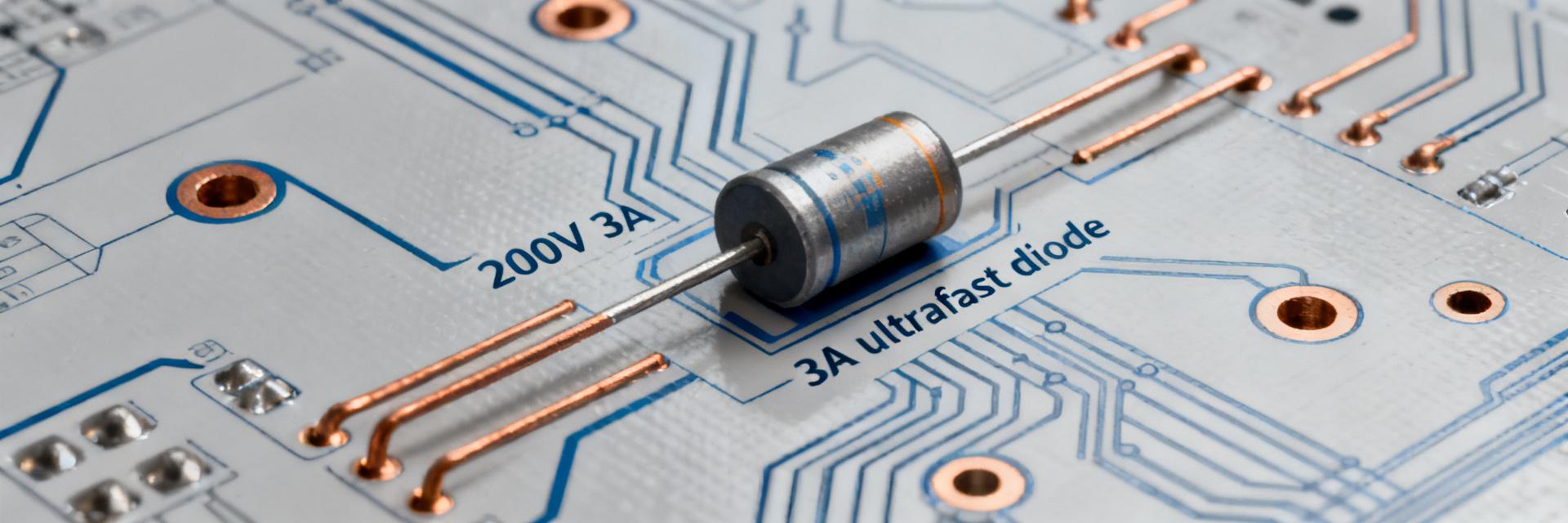
The MMBD914 is a small-signal, high-speed switching diode designed for clamping, level shifting, and signal steering. Engineers select this part when sub-microsecond response and a compact SOT-23 footprint are required for dense PCB layouts.
2. Electrical & Thermal Critical Limits
| Parameter | Symbol | Typical Value | Max Rating |
|---|---|---|---|
| Reverse Breakdown Voltage | V(BR)R | 100V | 100V |
| Peak Forward Surge Current | IFSM | 1.0A (1s) | 4.0A (1μs) |
| Reverse Recovery Time | trr | 4.0 ns | -- |
| Power Dissipation (25°C) | Pd | -- | 350 mW |
2.1 — Thermal Derating
Thermal resistance (RthJA) maps dissipation to board copper area. Calculate Pd = IF · VF(avg) and ensure junction temperature stays below 150°C. For repeated pulse events, verify the transient thermal impedance curve to prevent localized junction burnout.
3. Switching Metrics & Signal Integrity
The Reverse Recovery Time (trr) of 4ns is the primary selection driver for 10MHz+ nodes. Designers must prioritize low Junction Capacitance (Cj) for high-impedance signal paths to minimize frequency-dependent loading and signal distortion.
4. SOT-23 Footprint & Assembly
Extract pin numbering and land pattern tolerances directly from the mechanical drawing. Use a standard SOT-23 land pattern but optimize paste apertures to prevent "tombstoning"—a common defect for small-body components. Ensure the thermal path utilizes sufficient copper on Pin 3 (Cathode) for heat dissipation.
5.1 — Design Checklist
- Verify VR margin (Safety factor of 1.5x - 2x recommended).
- Confirm trr meets the system switching frequency requirements.
- Validate IFSM ratings for inrush or transient events.
- Bench-test VF and recovery waveforms at target operating temperature.
Common Questions (FAQ)
What are the typical MMBD914 switching characteristics to verify?
Focus on trr, storage time, and the recovery current waveform. Verify trr at your intended forward current (IF) and ensure recovery energy won't cause conduction into unintended nodes or cause ringing at high switching frequencies.
How should an engineer interpret reverse current and capacitance?
Treat IR and Cj as bias-dependent. For low-noise or high-impedance inputs, prioritize low IR (leakage); for high-speed signals, prioritize low Cj and check how it changes across the voltage range to estimate bandwidth impact.
What are quick troubleshooting steps if the diode fails?
Check for over-voltage transients exceeding VR, repeated surges beyond IFSM, and poor thermal relief on the PCB. Increase VR margin or improve copper area for thermal dissipation if overheating occurs.
Why use MMBD914 over general purpose diodes?
The MMBD914 is optimized for speed. While a general-purpose diode might handle the current, its slow recovery time (trr) would lead to excessive heat and signal corruption in high-frequency circuits.
Summary
Designers must balance absolute ratings (VR/IF) against switching characteristics (trr) and SOT-23 thermal constraints. Next steps: run margin checks, verify the land pattern, and bench-test recovery waveforms under real-world load conditions.