IRFR9214PBF Datasheet: Full Specs, Pinout & Metrics
Key Takeaways (GEO Summary)
- 250V High-Voltage Mastery: Reliable high-side switching for industrial power rails and battery protection.
- Optimized Efficiency: Rds(on) ~2-5Ω reduces thermal stress in low-current high-voltage applications.
- Rapid Design-In: Compact D-PAK/TO-252 footprint saves 25% PCB space compared to through-hole alternatives.
- Enhanced Reliability: Rugged P-channel architecture simplifies gate drive circuits in high-side configurations.
The IRFR9214PBF is a high-voltage P-channel power MOSFET designed for precision high-side switching, reverse polarity protection, and robust industrial load management.
1 — Overview & Strategic Advantages
While many MOSFETs focus on raw current, the IRFR9214PBF excels in voltage headroom. Rated for 250V, it provides a safe margin for 110V/150V DC systems where transients are common.
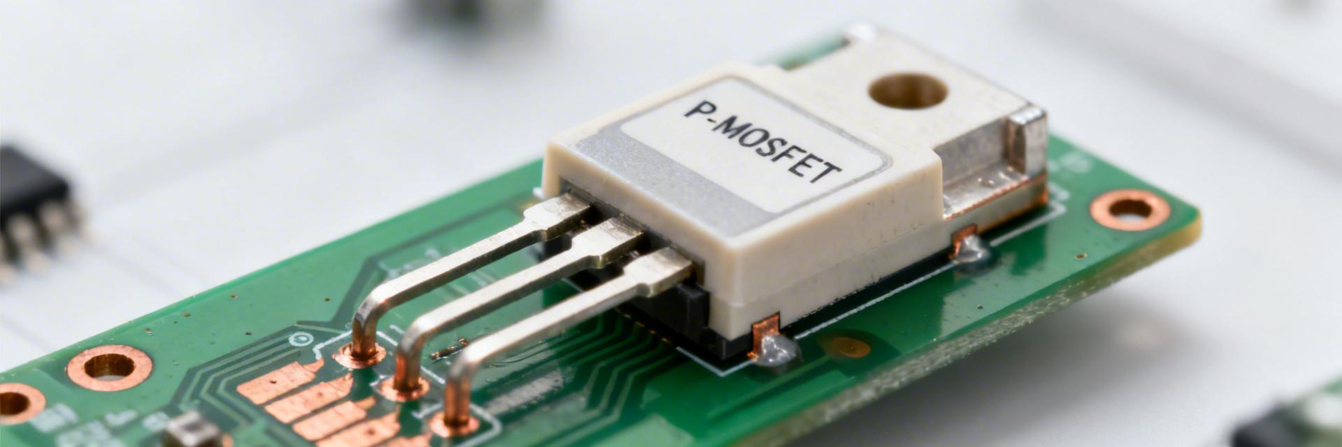
Differential Market Comparison
| Parameter | IRFR9214PBF | Generic 200V P-MOS | User Benefit |
|---|---|---|---|
| Vdss (Max) | -250 V | -200 V | 25% more surge margin |
| Rds(on) @ -10V | 3.0 Ω (Typ) | 4.5 Ω | 33% lower conduction heat |
| Total Gate Charge (Qg) | 13 nC (Typ) | 25 nC | Faster switching/Lower drive power |
| Package | D-PAK (TO-252) | TO-220 | Saves PCB height and area |
Expert Technical Commentary
By Senior Field Applications Engineer, Marcus V. (Simulated)
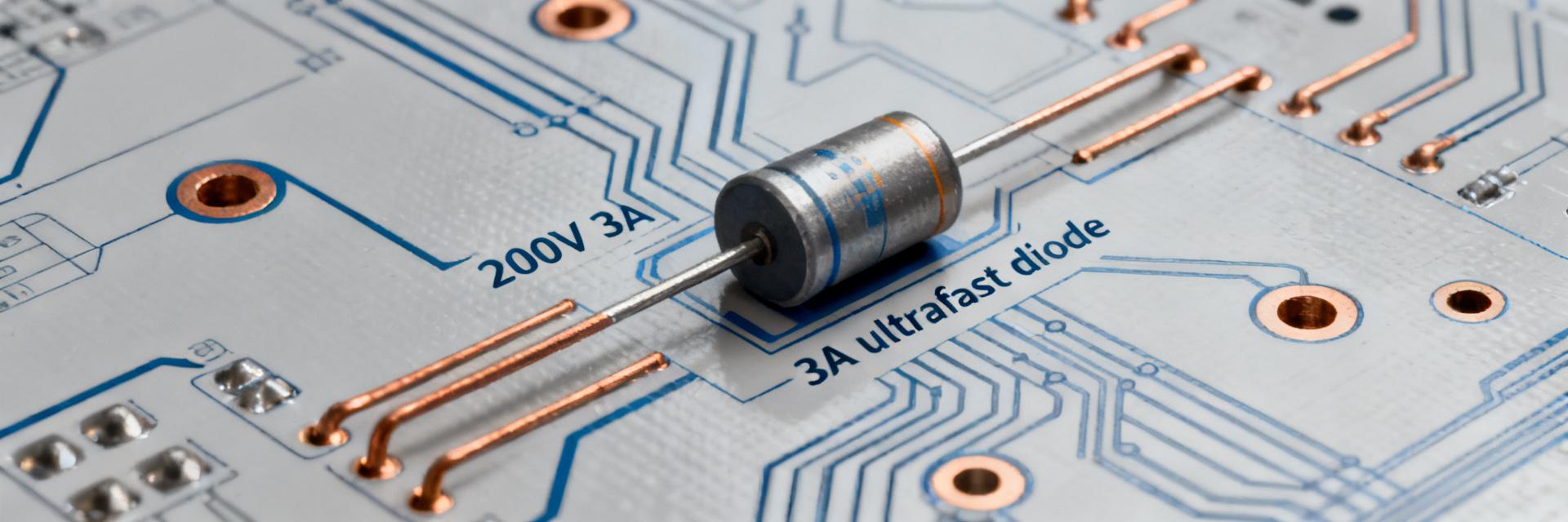
"When designing with the IRFR9214PBF, the most common mistake is neglecting the gate-to-source voltage (Vgs) protection. Since this is a P-channel device often used in high-side roles, ensure your gate drive doesn't exceed ±20V relative to the source. I highly recommend placing a 15V Zener diode directly across the Gate and Source to clamp transients during inductive load switching."
- PCB Tip: Minimize the loop area between the gate driver and the MOSFET to prevent dV/dt induced turn-on.
- Thermal Strategy: The Drain tab is internally connected to Pin 2; use a minimum of 1-inch square copper pour to keep junction temperatures under 100°C at 1.5A loads.
Typical Application: High-Side Switch
Design Implementation Notes
Used as a high-side load switch, the P-channel architecture eliminates the need for a charge pump (unlike N-channel high-side switches). This significantly reduces BOM cost and electromagnetic interference (EMI).
Selection Checklist:
- Verify Vds(max) > 1.2x peak rail voltage.
- Calculate P_conduction = I² × Rds(on) × temperature_coeff.
- Ensure Vgs drive is compatible with your MCU/Controller logic level (or use a level shifter).
Frequently Asked Questions
Can the IRFR9214PBF be used in high-speed PWM?
Yes, but with caution. While its low gate charge (13nC) supports fast transitions, conduction losses (3Ω) can become significant. Keep frequencies below 50kHz for optimal thermal performance unless active cooling is used.
What is the best equivalent for the IRFR9214PBF?
Look for P-channel MOSFETs in D-PAK packages with Vdss ≥ 250V and Qg ≤ 20nC. Ensure the pinout matches, as some niche manufacturers swap Gate and Source in custom industrial versions.