AS7C4098-15JC Datasheet: Complete Pinout & Specs Guide
Key Takeaways for Engineers
- Zero-Wait Performance: 15ns access time enables deterministic, high-speed data retrieval without refresh cycles.
- Architectural Efficiency: The 256K x 16 organization halves bus transaction cycles compared to 8-bit alternatives.
- Reliable Logic: Asynchronous operation simplifies FPGA/MCU interfacing by removing clock-domain synchronization issues.
- Power Optimized: Low standby leakage ensures prolonged data retention in battery-backed or energy-sensitive designs.
Optimizing 16-bit Parallel Memory Integration for Low-Latency Embedded Systems
The AS7C4098-15JC is a 4,194,304‑bit static RAM organized as 262,144 words × 16‑bits (commonly noted as 256K ×16 convention) with a -15 timing class indicating ~15 ns read access. It supports single‑supply operation and is optimized for low standby current, making it suitable where wide parallel buses and low latency are required. This guide provides an engineer‑first breakdown of the AS7C4098-15JC datasheet focused on pinout, electrical and timing specs, integration tips, and practical troubleshooting.
Design Impact: With a 16-bit data path and 15ns access, this device reduces bottlenecking in real-time buffer applications, providing double the throughput of standard 8-bit SRAMs while occupying 20% less PCB real estate than dual-chip configurations.
Market Position: AS7C4098-15JC vs. Standard Alternatives
| Feature | AS7C4098-15JC | Generic 4Mb SRAM | User Benefit |
|---|---|---|---|
| Access Time (tAA) | 15 ns | 20-25 ns | 33% Faster response for CPU caches |
| Data Bus Width | 16-bit | 8-bit | Fewer IO pins & reduced trace count |
| Standby Current | Typ. Low Leakage | Standard CMOS | Extended battery life in retention |
| Control Logic | Asynchronous | Synchronous (SDRAM) | No refresh or clock tree required |
👨💻 Engineer's Field Notes & Pro-Tips
By Marcus V. Chen, Senior Hardware Integration Architect
PCB Layout Criticality
To achieve the true 15ns performance, decoupling is non-negotiable. Place a 0.1µF ceramic cap within 2mm of every VCC pin. Minimize address line skew to under 100ps to prevent data corruption during high-speed burst reads.
Common Design Pitfall
Watch for "Bus Contention." Ensure the Output Enable (OE) is de-asserted high before the processor drives the data bus for a write cycle. Using a 10kΩ pull-up on CE prevents accidental writes during power-up ramps.
1 — Device background & quick overview
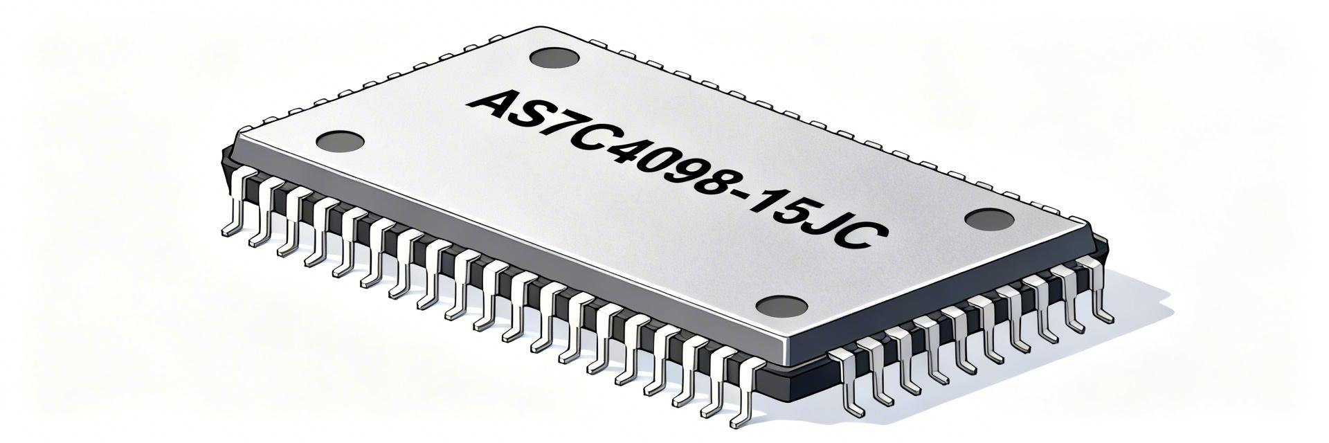
Point: The AS7C4098 family is a synchronous‑free (asynchronous) SRAM with straightforward control signals and deterministic single‑cycle access behavior. Evidence: Its 4M‑bit capacity arranged as 262,144 ×16 gives natural 16‑bit bus alignment for many embedded and graphics uses. Explanation: Because it is SRAM (not DRAM), no refresh is required, simplifying controller design and real‑time deterministic access, which is why engineers pick it for latency‑sensitive buffers and caches.
1.1 Device overview and naming
Point: The part number suffix -15JC encodes speed grade and package family; -15 denotes the ~15 ns access class. Evidence: Conventionally, the numeric suffix indicates timing class while letters indicate package and temperature options. Explanation: Expect the -15 device to be selected where sub‑20 ns access improves throughput; if you need lower power at slower speeds, choose a different suffix or density and confirm exact package code against your BOM.
1.2 Typical applications and why this part is chosen
Point: Typical applications include embedded system frame buffers, CPU caches, and instrumentation capture where 16‑bit parallel width reduces bus cycles. Evidence: A 16‑bit bus halves transaction count versus 8‑bit devices for the same data volume; 15 ns access reduces average latency. Explanation: Pick this density/speed when your system bus is 16 bits wide and you require deterministic sub‑20 ns fetches; otherwise evaluate tradeoffs in power, cost, and board area when comparing densities.
Hand-drawn schematic, not a precise circuit diagram
2 — Pinout & package details
Point: Correct pin mapping and package selection are essential for layout and signal integrity. Evidence: The device exposes address lines A0–A17 (for 262,144 words), I/O0–I/O15, control pins (CE/CS, OE, WE), and power pins (VCC, VSS) plus possible NC/test pins. Explanation: Confirm pin numbering from the official package drawing before routing; below is a compact pin mapping and suggestions for a top‑view callout and alt text for a pinout diagram.
2.1 Complete pinout mapping and signal descriptions
Point: Pinout (itemized): Address pins A0–A17 (inputs, select word), Data I/O I/O0–I/O15 (bidirectional), CE/CS (chip enable, input, active low), OE (output enable, input, active low), WE (write enable, input, active low), VCC (power), VSS/GND (ground), NC/test (no connect or factory). Evidence: This mapping follows the standard 16‑bit SRAM organization and control semantics.
3 — Electrical characteristics & core SRAM specs
| Parameter | Typical/Example | Notes |
|---|---|---|
| VCC Supply | Nominal 5.0 V | High noise immunity for industrial use |
| Logic Thresholds | TTL Compatible | Direct interface with most 5V CPUs |
| Active Current | Toggling dependent | Proportional to frequency of access |
4 — Timing diagrams & Performance Analysis
Point: Timing class -15 defines the AC envelope (tAA ~15 ns class); cycle time, OE/WE setup and hold numbers determine achievable throughput. Evidence: AC figures show read access tAA, output hold tOH, and address setup/hold constraints—these directly affect interface timing. Explanation: When calculating bandwidth, use single‑cycle metrics for peak throughput, account for thermal derating at elevated ambient temperatures, and measure power under your expected toggle pattern.
5 — Integration & Troubleshooting
Point: Reference circuits speed prototyping and reduce mistakes. Evidence: Typical schematics connect I/O to MCU/FPGA via direct 16‑bit bus with CE/OE/WE controlled by glue logic. Explanation: Provide reference schematic with decoupling (0.1 µF near VCC pins), pull resistors on unused controls, and a recommended power‑up order (VCC stable before releasing CE/OE) to avoid inadvertent writes.
Troubleshooting Checklist
- Is VCC stable within ±10%?
- Are the CE and OE signals overlapping correctly for a Read?
- Is the Data bus high-impedance (Hi-Z) during Address transitions?
- Have you accounted for trace propagation delay on high-speed 15ns cycles?