TIP122G datasheet analysis: real specs, limits & SOA
Core Thesis:
The TIP122G datasheet presents conservative maximum ratings that can mislead designers if read at face value. This article translates datasheet numbers into usable engineering limits so designers predict real behavior and avoid thermal or SOA surprises.
What You Will Learn:
Line-by-line decoding, practical formulas, test steps, and example calculations. This lets engineers size base drive, heatsinking, and pulse duty safely for low-side switching and motor-drive cases.
Quick Background: What TIP122G is and When to Use It
Device Family & Topology
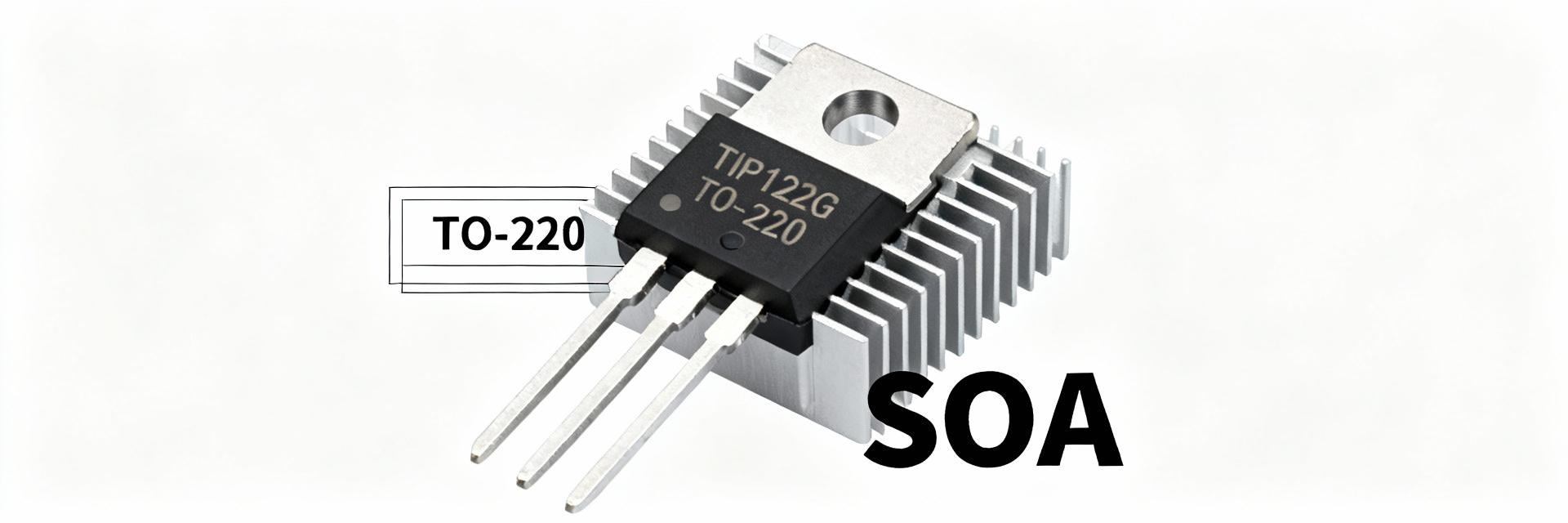
The device is an NPN Darlington power transistor in a TO-220 style package. Datasheet tables list VCEO near 100V, IC ratings up to 5A, and Darlington characteristics such as high hFE and elevated VCE(sat). This means very high current gain and easy logic drive but higher saturation voltage and thermal penalties compared with single BJTs or MOSFETs.
Typical Application Envelope
Darlingtons suit low-side switching and buffering but are poor for high-efficiency switching or heavy linear dissipation. High VCE(sat) and large Pd per device create significant heat at several amps. Use them for relay drivers, hobby motors, or buffering logic outputs; choose a MOSFET for high-efficiency switching.
Datasheet Electrical Specs: Decode the Numbers
VCEO Rating
Collector-Emitter Voltage: 100V Max
IC Current
Continuous Current: 5A Max
hFE Gain
DC Current Gain: 1000 Typ.
Translating Specs to Design Constraints
Convert tabular numbers into design formulas: P = VCE × IC. For example, a VCE(sat) = 2V at IC = 2A yields ~4W of static dissipation. Ensure base current and drive timing are included in designs to avoid saturation-related heating, as saturating Darlingtons require specific base current margins.
Safe Operating Area (SOA) & Second-Breakdown
SOA plots show allowable VCE–IC regions by pulse duration. Second breakdown is a localized failure at high VCE and moderate IC, often invisible until destruction. Darlingtons are particularly susceptible because they combine two junctions and internal stress.
Plot Interpretation
- ◈ Identify pulse width matching your case.
- ◈ Derate for ambient temperature.
Risk Mitigation
- ◈ Avoid the steep SOA boundaries.
- ◈ Include a 20-30% safety margin.
Thermal Limits & Heatsink Calculations
Junction temperature (Tj) drives allowable dissipation. Calculate via the thermal resistance chain:
Tj = Ta + Pd × (RthJC + RthCS + RthSA)
Example: 4W of Pd with a total resistance of 10°C/W raises the junction by ~40°C. Ensure Tj remains below Tmax (usually 150°C) with significant margin. Use large copper areas, thermal vias, and correct mounting torque to minimize RthSA.
Application Scenarios
Switching (Motor Drive)
For a 12V motor drawing 3A, if VCE(sat) ≈ 2V, conduction loss is ≈6W. This requires substantial heatsinking or pulsed duty. Ensure base drive pulses are adequate to keep the transistor fully saturated.
Linear/Analog Operation
A 12V drop at 2A equals 24W, which is far above comfortable Pd. Avoid series-pass linear applications unless you add emitter resistors, active cooling, or distribute dissipation across multiple devices.
Validation & Design Mitigations
Lab Test Checklist
- ✓ Pulsed SOA tests with controlled duty cycles.
- ✓ Thermal ramp monitoring using infrared imaging.
- ✓ VCE(sat) checks under full load conditions.
Design Mitigations
- ★ Hardware: Snubbers or series resistors for protection.
- ★ Firmware: Soft-start PWM and thermal shutdown logic.
- ★ Paralleling: Use emitter resistors for current sharing.
Key Summary
- • The TIP122G datasheet lists nominal limits; always convert curves into numeric safe points for your specific pulse duration and ambient conditions.
- • Extract VCEO, IC, VCE(sat), and thermal resistances early to size heatsinking and base drive correctly.
- • Apply at least 20–30% margin to SOA limits and consider MOSFETs if thermal or efficiency targets are extremely tight.