1201M2S3AV2KG2 Fiche technique Approfondi : Spécifications et empreinte
The goal of this deep dive is to extract the measurable, design‑critical information engineers need from the component datasheet and convert it into a verified PCB footprint and validation plan. This introduction focuses on how to read the datasheet, prioritize sections, and capture the electrical and mechanical parameters that directly drive pad geometry, thermal strategy, and assembly constraints.
1 — Background & Typical Applications

Device category & functional overview
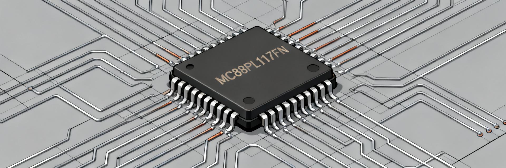
Point: Determine the component class and intended application spaces before committing to a footprint. Evidence: The datasheet title, ordering codes, and functional block diagram reveal the 1201M2S3AV2KG2 is a subminiature slide switch. Explanation: Identifying the device class informs expected tolerances and mounting robustness for applications like IoT modules and industrial controllers.
Key datasheet sections to prioritize
Point: Prioritize electrical characteristics, mechanical dimensions, and land patterns. Evidence: These sections contain pin count, pitch, and max height. Explanation: Extract pin numbering and nominal dimensions to create a checklist for CAD primitives, ensuring enclosure clearance and assembly compatibility.
2 — 1201M2S3AV2KG2 datasheet: Electrical & Mechanical Breakdown
Electrical specifications to extract and verify
Point: Extract absolute maximum ratings and operating ranges. Evidence: Datasheet tables for maximum conditions guide power budgeting. Explanation: Translate these into system constraints, defining decoupling and protection requirements.
| Field | Value (from datasheet) | Design action |
|---|---|---|
| Absolute Vmax | [20V DC/AC] | Clamp/protection, margin |
| Operating V | [0.4 VA max] | Supply net assignment |
| Max I or Pd | [Record per Temp] | Copper pour, thermal vias |
| Timing / tR, tF | [Contact Bounce] | Signal integrity, debounce |
3 — 1201M2S3AV2KG2 footprint: PCB Land Pattern & 3D Model
IPC-compliant land pattern translation
| Item | Typical value |
|---|---|
| Pad center-to-center | [Verify Pitch: 2.54mm/5.08mm] |
| Pad width / length | [Lead size + Solder fillet] |
| Paste aperture | 70–90% of pad area |
| Mask openings | 0.05-0.1mm clearance |
4 — Layout Integration & Manufacturing
Thermal management and assembly
Point: Determine thermal strategy based on θJA. Evidence: Datasheet thermal resistance indicates heat routing needs. Explanation: Place thermal via arrays under pads if power dissipation exceeds passive limits. Configure stencil apertures to prevent tombstoning during reflow.
5 — Validation Checklist
- FAI: Inspect solder fillet quality and placement accuracy against datum.
- Electrical: Continuity and insulation resistance per datasheet specs.
- Mechanical: Verify height clearance and actuator alignment for enclosure fit.
- Traceability: Document pad dimensions and pitch vs datasheet drawing.
Frequently Asked Questions
What are the critical datasheet items to verify before creating the footprint?
Verify absolute maximum ratings, recommended operating conditions, pin-out and pin numbering, package outline with tolerances, recommended land pattern, and any assembly notes such as soldering temperature limits.
How do I decide pad size and paste aperture from the datasheet?
Base pad size on lead width and expected fillet, choosing a pad length that supports stable placement and fillet formation. Use paste aperture reductions (typically 70–90% of the pad) to control solder volume.
Which tests validate that a footprint meets datasheet requirements?
Run first article inspection checks (placement, fillet shape), electrical tests under nominal operating conditions, thermal measurement under worst-case power, and mechanical fit checks for height and mating interfaces.
How is thermal management handled for 1201M2S3AV2KG2?
If power dissipation exceeds board spreading capability, place a thermal via array under pads following a grid pattern (0.6–1.0 mm spacing) tied to internal copper pours; define measurement points near the hottest expected node.
Summary
Accurate interpretation of the 1201M2S3AV2KG2 datasheet ensures reliable assembly and long-term performance. By systematically extracting mechanical and electrical data, designers can create IPC-compliant footprints that minimize rework and optimize manufacturing yield.