MN103SF65GYD Hoja de datos completa y guía general de conexiones
This guide condenses the MN103SF65GYD datasheet into a compact, engineer-focused reference for rapid design decisions. By focusing on measurable electrical limits and precise pin assignments, firmware and hardware teams can shorten prototype cycles and ensure long-term reliability.
Background & Key Use Cases
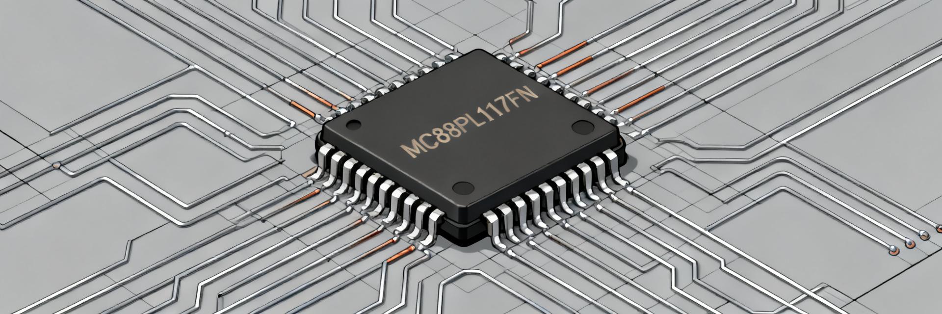
The MN103SF65GYD is a versatile embedded controller designed for low-to-mid-range sensor and power-management applications. Engineers select this IC for its compact footprint and integrated peripherals in cost-sensitive industrial designs.
Pinout & Functional Grouping
| Pin # | Pin Name | Function | Type |
|---|---|---|---|
| 1 | VCC | Primary supply rail | Power |
| 2 | GND | Ground return | Ground |
| 3 | PA0 / UART_TX | UART transmit / GPIO | I/O |
| 4 | PA1 / UART_RX | UART receive / GPIO | I/O |
| 5 | ADC_IN0 | Analog input channel 0 | Analog |
| 6 | RESET | Reset input (active low) | Control |
| 7 | XTAL_IN | External crystal input | Clock |
| 8 | NC | No connect / reserved | — |
Core Implementation Guidelines
Success with the MN103SF65GYD depends on respecting thermal and electrical boundaries. Key practices include placing 0.1µF decoupling caps within 2mm of VCC pins and isolating analog paths from digital return currents to maintain ADC precision.
Common Questions
What is the MN103SF65GYD pinout for UART/SPI?
What supply voltages does MN103SF65GYD support?
How to add decoupling caps for MN103SF65GYD?
What are the recommended PCB layout tips?
Source: MN103SF65GYD Technical Documentation (Manufacturer Official Reference).