ورق بيانات RY8126 DC-DC Buck تحليل عميق وشرح المعايير الأساسية
Datasheet curves for switching converters directly determine board area, thermal margin, and system efficiency; understanding how those numbers map to real-world behavior avoids costly re-spins. This guide translates datasheet tables and graphs into design-impact statements so power engineers can plan PCB area, thermal budget, and component selection from day one. The main keyword RY8126 appears as a focal device for these steps.
1 — Background: What the RY8126 DC-DC Buck Is and Where It Fits
1.1 — High-level feature summary
The RY8126 is a synchronous step-down regulator used for point-of-load conversion. Consult the datasheet tables for exact VIN range, VOUT range, and maximum output current. These figures determine inductor RMS current and thermal needs before layout.
1.2 — Target applications & comparative positioning
The device targets compact, efficient power conversion in IoT and consumer systems. Choose this family when you need a compact DC-DC Buck with competitive efficiency for specific amperage ranges where thermal margin is critical.
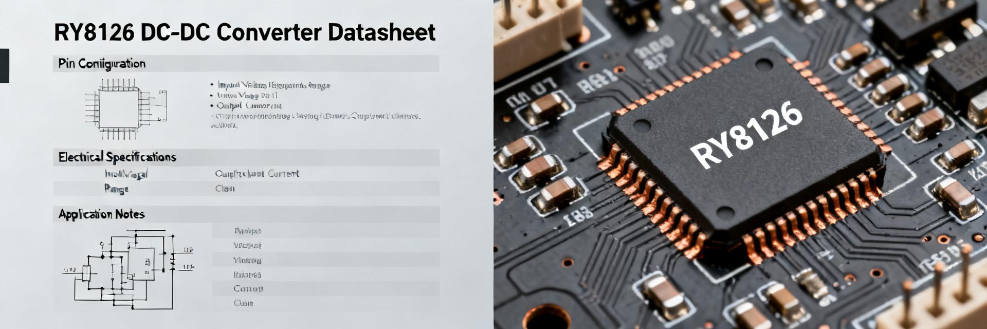
2 — Pinout, Packaging & Absolute Ratings
2.1 — Pin functions and recommended footprint
| Pin Name | Function | Layout Priority |
|---|---|---|
| VIN | Input Voltage Supply | Critical: Place input cap immediately adjacent |
| SW | Switching Node | Minimize area to reduce EMI |
| FB | Feedback Input | Route away from SW node; keep trace short |
| GND/EPAD | Ground & Thermal Pad | Direct connection to ground plane via multiple vias |
3 — Key Electrical Specs: Efficiency & Thermal
3.1 — Efficiency and Power Loss
Efficiency curves indicate how much input power becomes heat. Use the formula P_loss = P_out * (1/η - 1). For the RY8126, use θJA from the thermal table to estimate PCB temperature rise: ΔT = P_loss * θJA.
3.2 — Regulation & Transient Response
Regulation plots define output ripple. If transient overshoot exceeds your system spec, increase output capacitance (Cout) or adjust the ESR according to the datasheet's compensation guidelines.
4 — Design Integration: BOM & Layout
4.1 — Component Selection Checklist
- Inductor: Ensure Isat > peak current; ΔI_L should be 20–40% of Iout.
- Capacitors: Must meet rated RMS current and low-ESR requirements.
- Feedback: Use 1% precision resistors for stable VOUT regulation.
4.2 — PCB Layout Best Practices
Place input capacitor pads immediately at VIN/GND pins. Tie the exposed pad to a large ground plane to improve thermal spreading and lower the junction temperature.
5 — Testing & Troubleshooting
5.1 — Bench Test Plan
Validate behavior with a supply ramp, no-load startup, and transient step tests. Compare your switch-node (SW) waveforms with the datasheet examples to ensure no excessive ringing or instability exists.
Summary
- Verify absolute ratings (VIN, VSW, Tj) to set safety margins for RY8126.
- Calculate power loss and size copper pours to manage ΔT effectively.
- Follow the recommended layout for thermal relief and EMI control.
FAQ
What VIN range should I use for RY8126 to maximize efficiency?
Refer to the datasheet recommended operating conditions table for the permitted VIN range and use the efficiency-vs-VIN graph to pick the VIN that yields peak efficiency at your expected load. Avoid running VIN at the extremes of the absolute maximum table to maintain thermal and reliability margin.
How do I interpret the RY8126 transient response graph for output capacitor selection?
Read the datasheet transient plot to see ΔV for a specified load step and time. If your measured transient exceeds allowable deviation, increase output capacitance or adjust ESR per the datasheet compensation guidance until the transient meets spec, then re-run bench step tests to validate.
Which PCB thermal measures are most effective with the RY8126?
Start with an exposed pad tied to multiple thermal vias into a ground plane, use wide copper pours on top and bottom, and add vias directly under the pad per the datasheet layout recommendation. Estimate temperature rise from P_loss and θJA and iterate copper area until the predicted ΔT is within limits.
What is the primary indicator of inductor saturation in an RY8126 design?
Look for a sharp, non-linear increase in peak current on the switch-node (SW) waveform or excessive output ripple. Ensure the inductor's saturation current (Isat) is 20-30% higher than the calculated peak current to prevent thermal runaway.